I’ve compiled this guide for the 74HC595 shift register to help engineers like you. Here, you’ll find the 74HC595 pinout diagram, detailed 74HC595 pin configuration, and key technical details from Texas Instruments. Expect clear pin descriptions, functional block diagrams, and package layouts. All data comes from the official datasheet, ensuring accuracy for your designs.
1. 74HC595 Pinout Diagram
The 74HC595 pinout diagram shows the pin assignments for this 8-bit shift register. I’ve included a placeholder below for the diagram, sourced from the datasheet.
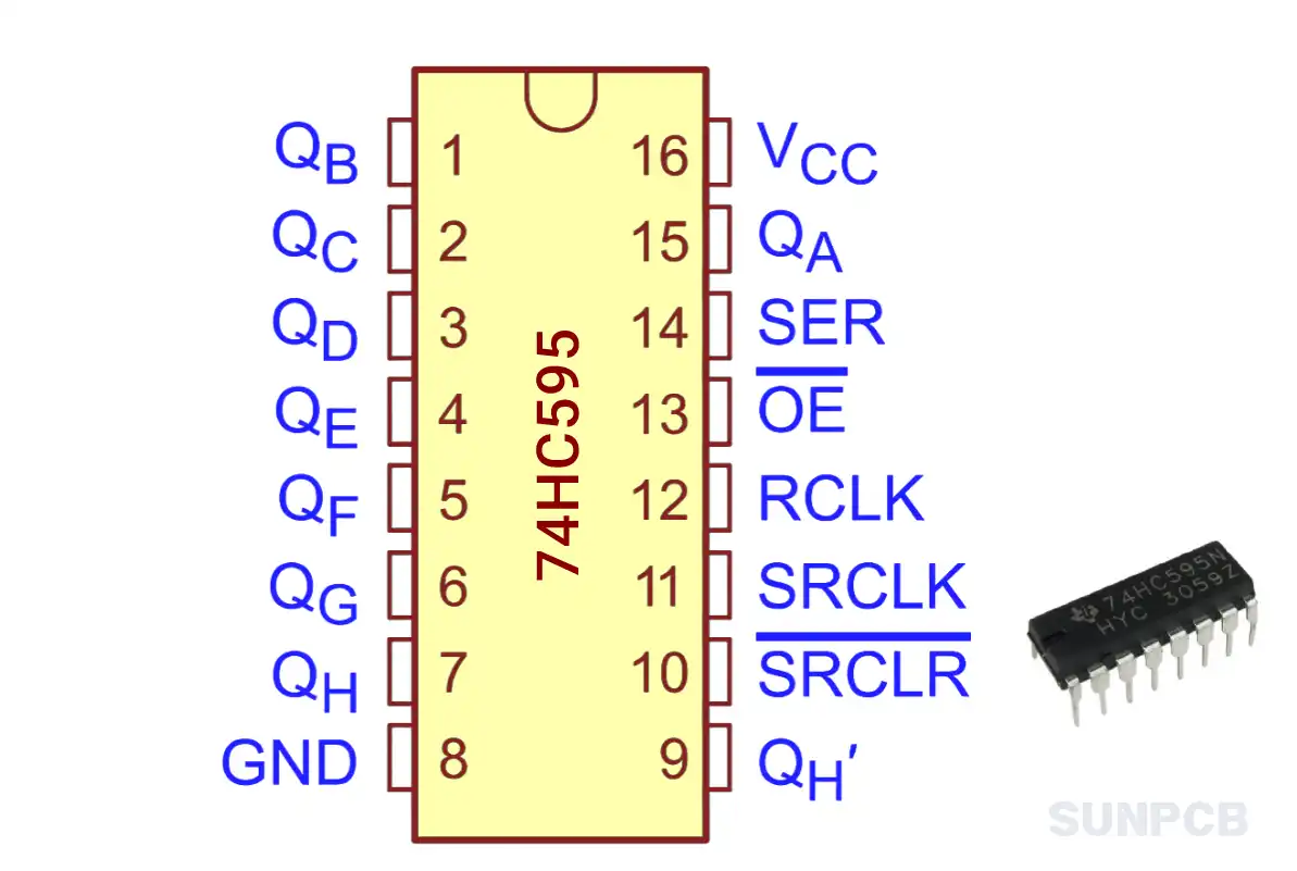
Figure: 74HC595 Pinout Diagram (Page 3/42)
![]() 74HC595 pinout diagram pdf download (P3/P42)
74HC595 pinout diagram pdf download (P3/P42)
2. 74HC595 Pin Configuration and Description
The 74HC595 pin configuration table lists all 16 pins for the SOIC, PDIP, SSOP, or TSSOP packages. Each pin’s function is detailed for your reference.
| Pin# | Pin Name | I/O | Pinout Description |
|---|---|---|---|
| 1 | Q_B | O | Q_B Output: Parallel output for bit B of the shift register. |
| 2 | Q_C | O | Q_C Output: Parallel output for bit C of the shift register. |
| 3 | Q_D | O | Q_D Output: Parallel output for bit D of the shift register. |
| 4 | Q_E | O | Q_E Output: Parallel output for bit E of the shift register. |
| 5 | Q_F | O | Q_F Output: Parallel output for bit F of the shift register. |
| 6 | Q_G | O | Q_G Output: Parallel output for bit G of the shift register. |
| 7 | Q_H | O | Q_H Output: Parallel output for bit H of the shift register. |
| 8 | GND | - | Ground Pin: Connect to system ground. |
| 9 | Q_H' | O | Q_H' Output: Serial output for cascading multiple shift registers. |
| 10 | SRCLR | I | Shift Register Clear Input: Active-low, clears the shift register when low. |
| 11 | SRCLK | I | Shift Register Clock Input: Shifts data on rising edge. |
| 12 | RCLK | I | Storage Register Clock Input: Latches shift register data to outputs on rising edge. |
| 13 | OE | I | Output Enable: Active-low, enables parallel outputs when low. |
| 14 | SER | I | Serial Data Input: Accepts serial data for the shift register. |
| 15 | Q_A | O | Q_A Output: Parallel output for bit A of the shift register. |
| 16 | V_CC | - | Power Pin: Supply voltage, typically 2V to 6V. |
3. 74HC595 Functional Block Diagram
The 74HC595 block diagram illustrates the internal structure of this shift register. Below, I summarize its key components, found on page 8 of the datasheet.
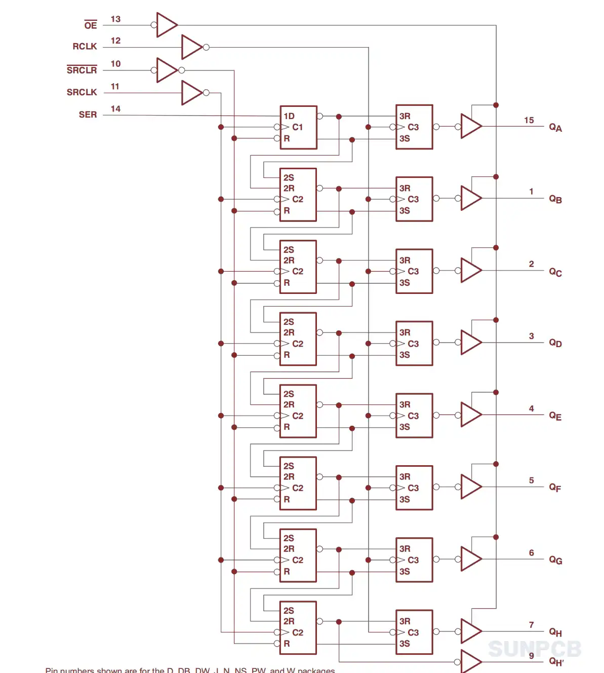
- Shift Register: 8-bit serial-in, parallel-out register for data shifting.
- Storage Register: Latches shift register data for parallel outputs.
- Output Enable: Controls output states, active-low.
- Serial Output: Enables cascading for multiple devices.
![]() 74HC595 functional block diagram pdf download (P8/P42)
74HC595 functional block diagram pdf download (P8/P42)
4. 74HC595 TI Overview
4.1 Description
The 74HC595 is an 8-bit shift register with a storage register and 3-state outputs. It’s designed for serial-to-parallel data conversion.
4.2 Overview
The 74HC595 devices contain an 8-bit serial-in, parallel-out shift register that feeds an 8-bit D-type storage register. The storage register has parallel 3-state outputs. Separate clocks are provided for both the shift and storage register. The shift register has a direct overriding clear (SRCLR) input, serial (SER) input, and serial outputs for cascading. When the output-enable (OE) input is high, the outputs are in the high-impedance state.
4.3 Features
- 8-bit serial-in, parallel-out shift register with storage register.
- Wide operating voltage range of 2V to 6V.
- High-current 3-state outputs can drive up to 15 LSTTL loads.
- Low power consumption, 80-µA max ICC.
- Typical tpd = 13 ns at 5V.
- ±6-mA output drive at 5V.
- Low input current of 1 µA max.
- Shift register has direct clear.
These features make the 74HC595 ideal for low-power, high-speed applications. Note the direct clear function, wich ensures reliable data reset.
4.4 Applications
LED drivers; Motor control; Display drivers; General-purpose logic.
5. 74HC595 FAQs and Tips
Below are common questions and tips for the 74HC595, addressing typical engineer concerns.
Q: What is the purpose of the OE pin?
A: The Output Enable pin controls the 3-state outputs. When low, outputs are active; when high, they’re in high-impedance state.
Q: Can I cascade multiple 74HC595s?
A: Yes, connect the Q_H' output of one to the SER input of the next for serial data transfer.
Q: What voltage range does it support?
A: The 74HC595 operates from 2V to 6V, ideal for various logic levels.
Q: How do I clear the shift register?
A: Pull the SRCLR pin low to reset the shift register data.
Q: What’s the max clock frequency?
A: At 5V, it’s typically 31 MHz, but check timing requirements for your setup.
Q: Why are outputs not updating?
A: Ensure RCLK is pulsed to latch shift register data to outputs.
Q: Is it suitable for LED driving?
A: Yes, its high-current outputs can drive LEDs efficiently.
Q: What’s the power consumption?
A: Max ICC is 80 µA, making it low-power for battery applications.
Q: What is the 74HC595 IC pinout?
A: The 74HC595 IC pinout includes 16 pins: SER (serial input), SRCLK (shift clock), RCLK (storage clock), OE (output enable), SRCLR (clear), Q_A to Q_H (parallel outputs), Q_H' (serial output), V_CC, and GND. Refer to the pin configuration table for details.
Q: How does the 74HC595 pinout work with Arduino?
A: For the 74HC595 pinout Arduino setup, connect SER to a digital pin (e.g., pin 11), SRCLK to another (e.g., pin 12), and RCLK to a third (e.g., pin 8). OE ties to GND for active outputs, and SRCLR to V_CC to disable clearing. Q_A to Q_H drive outputs like LEDs.
Q: What is the 74HC595 shift register pinout?
A: The 74HC595 shift register pinout features pins for serial data (SER), shift clock (SRCLK), storage clock (RCLK), clear (SRCLR), and output enable (OE). Parallel outputs are Q_A to Q_H, with Q_H' for cascading and V_CC/GND for power.
Q: How is the shift register 74HC595 pinout configured?
A: The shift register 74HC595 pinout includes SER (pin 14) for data input, SRCLK (pin 11) for shifting, and RCLK (pin 12) for latching. SRCLR (pin 10) clears data, OE (pin 13) controls outputs, and Q_A to Q_H (pins 15, 1-7) provide parallel outputs.
Q: What is the 74HC595 SMD pinout?
A: The 74HC595 SMD pinout for SOIC, SSOP, or TSSOP packages matches the DIP version: 16 pins with SER (pin 14), SRCLK (pin 11), RCLK (pin 12), OE (pin 13), SRCLR (pin 10), Q_A to Q_H (pins 15, 1-7), Q_H' (pin 9), V_CC (pin 16), and GND (pin 8).
Tips:
- Use decoupling capacitors near V_CC to reduce noise.
- Ensure SRCLR is high during normal operation to avoid accidental clears.
- Connect unused inputs to V_CC or GND to prevent floating states.
- For cascading, synchronize SRCLK across devices.
- Check output drive limits (±6 mA at 5V) for heavy loads.