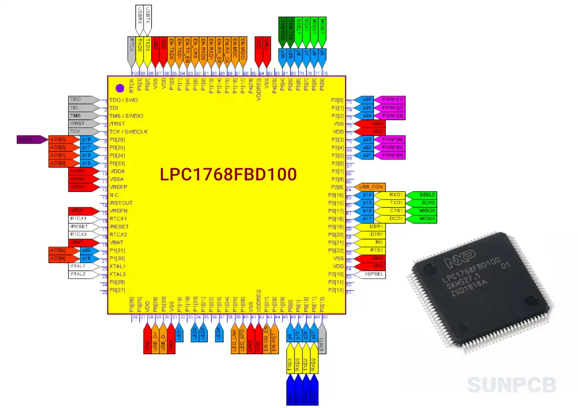
1. LPC1768FBD100 Pinout Diagram
The LPC1768FBD100 pinout diagram illustrates the pin layout for the 100-pin LQFP package.
2. LPC1768FBD100 Pin Configuration and Description
The LPC1768FBD100 pin configuration and LPC1768FBD100 pin description are listed below for all 100 pins of the LQFP-100 package, as per the official datasheet Section 7.2, Table 5.
| Pin Number | Symbol | Type | Description |
|---|---|---|---|
| 1 | TDO/SWO | O | TDO — Test Data out for JTAG interface. SWO — Serial wire trace output. |
| 2 | TDI | I | TDI — Test Data in for JTAG interface. |
| 3 | TMS/SWDIO | I I/O |
TMS — Test Mode Select for JTAG interface. SWDIO — Serial wire debug data input/output. |
| 4 | TRST | I | TRST — Test Reset for JTAG interface. |
| 5 | TCK/SWDCLK | I | TCK — Test Clock for JTAG interface. SWDCLK — Serial wire clock. |
| 6 | P0[26]/AD0[3]/AOUT/RXD3 | I/O I O I |
P0[26] — General purpose digital input/output pin. AD0[3] — A/D converter 0, input 3. AOUT — DAC output (LPC1769/68/67/66/65/63 only). RXD3 — Receiver input for UART3. |
| 7 | P0[25]/AD0[2]/I2SRX_SDA/TXD3 | I/O I I/O O |
P0[25] — General purpose digital input/output pin. AD0[2] — A/D converter 0, input 2. I2SRX_SDA — Receive data. It is driven by the transmitter and read by the receiver. Corresponds to the signal SD in the I2S-bus specification. (LPC1769/68/67/66/65/63 only). TXD3 — Transmitter output for UART3. |
| 8 | P0[24]/AD0[1]/I2SRX_WS/CAP3[1] | I/O I I/O I |
P0[24] — General purpose digital input/output pin. AD0[1] — A/D converter 0, input 1. I2SRX_WS — Receive Word Select. It is driven by the master and received by the slave. Corresponds to the signal WS in the I2S-bus specification. (LPC1769/68/67/66/65/63 only). CAP3[1] — Capture input for Timer 3, channel 1. |
| 9 | P0[23]/AD0[0]/I2SRX_CLK/CAP3[0] | I/O I I/O I |
P0[23] — General purpose digital input/output pin. AD0[0] — A/D converter 0, input 0. I2SRX_CLK — Receive Clock. It is driven by the master and received by the slave. Corresponds to the signal SCK in the I2S-bus specification. (LPC1769/68/67/66/65/63 only). CAP3[0] — Capture input for Timer 3, channel 0. |
| 10 | VDDA | I | analog 3.3 V pad supply voltage: This should be nominally the same voltage as VDD(3V3) but should be isolated to minimize noise and error. This voltage is used to power the ADC and DAC. This pin should be tied to 3.3 V if the ADC and DAC are not used. |
| 11 | VSSA | I | analog ground: 0 V reference. This should nominally be the same voltage as VSS, but should be isolated to minimize noise and error. |
| 12 | VREFP | I | ADC positive reference voltage: This should be nominally the same voltage as VDDA but should be isolated to minimize noise and error. Level on this pin is used as a reference for ADC and DAC. This pin should be tied to 3.3 V if the ADC and DAC are not used. |
| 13 | n.c. | - | not connected. |
| 14 | RSTOUT | O | RSTOUT — This is a 3.3 V pin. LOW on this pin indicates the microcontroller being in Reset state. |
| 15 | VREFN | I | ADC negative reference voltage: This should be nominally the same voltage as VSS but should be isolated to minimize noise and error. Level on this pin is used as a reference for ADC and DAC. |
| 16 | RTCX1 | I | Input to the RTC oscillator circuit. |
| 17 | RESET | I | External reset input: A LOW-going pulse as short as 50 ns on this pin resets the device, causing I/O ports and peripherals to take on their default states, and processor execution to begin at address 0. TTL with hysteresis, 5 V tolerant. |
| 18 | RTCX2 | O | Output from the RTC oscillator circuit. |
| 19 | VBAT | I | RTC pin power supply: 3.3 V on this pin supplies the power to the RTC peripheral. |
| 20 | P1[31]/SCK1/AD0[5] | I/O I/O I |
P1[31] — General purpose digital input/output pin. SCK1 — Serial Clock for SSP1. AD0[5] — A/D converter 0, input 5. |
| 21 | P1[30]/VBUS/AD0[4] | I/O I I |
P1[30] — General purpose digital input/output pin. VBUS — Monitors the presence of USB bus power. (LPC1769/68/66/65/64 only). Note: This signal must be HIGH for USB reset to occur. AD0[4] — A/D converter 0, input 4. |
| 22 | XTAL1 | I | Input to the oscillator circuit and internal clock generator circuits. |
| 23 | XTAL2 | O | Output from the oscillator amplifier. |
| 24 | P0[28]/SCL0/USB_SCL | I/O I/O I/O |
P0[28] — General purpose digital input/output pin. Output is open-drain. SCL0 — I2C0 clock input/output. Open-drain output (for I2C-bus compliance). USB_SCL — USB port I2C serial clock (OTG transceiver, LPC1769/68/66/65 only). |
| 25 | P0[27]/SDA0/USB_SDA | I/O I/O I/O |
P0[27] — General purpose digital input/output pin. Output is open-drain. SDA0 — I2C0 data input/output. Open-drain output (for I2C-bus compliance). USB_SDA — USB port I2C serial data (OTG transceiver, LPC1769/68/66/65 only). |
| 26 | P3[26]/STCLK/MAT0[1]/PWM1[3] | I/O I O O |
P3[26] — General purpose digital input/output pin. STCLK — System tick timer clock input. The maximum STCLK frequency is 1/4 of the Arm processor clock frequency CCLK. MAT0[1] — Match output for Timer 0, channel 1. PWM1[3] — Pulse Width Modulator 1, output 3. |
| 27 | P3[25]/MAT0[0]/PWM1[2] | I/O O O |
P3[25] — General purpose digital input/output pin. MAT0[0] — Match output for Timer 0, channel 0. PWM1[2] — Pulse Width Modulator 1, output 2. |
| 28 | VDD(3V3) | I | 3.3 V supply voltage: This is the power supply voltage for the I/O ports. |
| 29 | P0[29]/USB_D+ | I/O I/O |
P0[29] — General purpose digital input/output pin. USB_D+ — USB bidirectional D+ line. (LPC1769/68/66/65/64 only). |
| 30 | P0[30]/USB_D- | I/O I/O |
P0[30] — General purpose digital input/output pin. USB_D- — USB bidirectional D- line. (LPC1769/68/66/65/64 only). |
| 31 | VSS | I | ground: 0 V reference. |
| 32 | P1[18]/USB_UP_LED/PWM1[1]/CAP1[0] | I/O O O I |
P1[18] — General purpose digital input/output pin. USB_UP_LED — USB GoodLink LED indicator. It is LOW when the device is configured (non-control endpoints enabled), or when the host is enabled and has detected a device on the bus. It is HIGH when the device is not configured, or when host is enabled and has not detected a device on the bus, or during global suspend. It transitions between LOW and HIGH (flashes) when the host is enabled and detects activity on the bus. (LPC1769/68/66/65/64 only). PWM1[1] — Pulse Width Modulator 1, channel 1 output. CAP1[0] — Capture input for Timer 1, channel 0. |
| 33 | P1[19]/MCOA0/USB_PPWR/CAP1[1] | I/O O O I |
P1[19] — General purpose digital input/output pin. MCOA0 — Motor control PWM channel 0, output A. USB_PPWR — Port Power enable signal for USB port. (LPC1769/68/66/65 only). CAP1[1] — Capture input for Timer 1, channel 1. |
| 34 | P1[20]/MCI0/PWM1[2]/SCK0 | I/O I O I/O |
P1[20] — General purpose digital input/output pin. MCI0 — Motor control PWM channel 0, input. Also Quadrature Encoder Interface PHA input. PWM1[2] — Pulse Width Modulator 1, channel 2 output. SCK0 — Serial clock for SSP0. |
| 35 | P1[21]/MCABORT/PWM1[3]/SSEL0 | I/O O O I/O |
P1[21] — General purpose digital input/output pin. MCABORT — Motor control PWM, LOW-active fast abort. PWM1[3] — Pulse Width Modulator 1, channel 3 output. SSEL0 — Slave Select for SSP0. |
| 36 | P1[22]/MCOB0/USB_PWRD/MAT1[0] | I/O O I O |
P1[22] — General purpose digital input/output pin. MCOB0 — Motor control PWM channel 0, output B. USB_PWRD — Power Status for USB port (host power switch, LPC1769/68/66/65 only). MAT1[0] — Match output for Timer 1, channel 0. |
| 37 | P1[23]/MCI1/PWM1[4]/MISO0 | I/O I O I/O |
P1[23] — General purpose digital input/output pin. MCI1 — Motor control PWM channel 1, input. Also Quadrature Encoder Interface PHB input. PWM1[4] — Pulse Width Modulator 1, channel 4 output. MISO0 — Master In Slave Out for SSP0. |
| 38 | P1[24]/MCI2/PWM1[5]/MOSI0 | I/O I O I/O |
P1[24] — General purpose digital input/output pin. MCI2 — Motor control PWM channel 2, input. Also Quadrature Encoder Interface INDEX input. PWM1[5] — Pulse Width Modulator 1, channel 5 output. MOSI0 — Master Out Slave in for SSP0. |
| 39 | P1[25]/MCOA1/MAT1[1] | I/O O O |
P1[25] — General purpose digital input/output pin. MCOA1 — Motor control PWM channel 1, output A. MAT1[1] — Match output for Timer 1, channel 1. |
| 40 | P1[26]/MCOB1/PWM1[6]/CAP0[0] | I/O O O I |
P1[26] — General purpose digital input/output pin. MCOB1 — Motor control PWM channel 1, output B. PWM1[6] — Pulse Width Modulator 1, channel 6 output. CAP0[0] — Capture input for Timer 0, channel 0. |
| 41 | VSS | I | ground: 0 V reference. |
| 42 | VDD(REG)(3V3) | I | 3.3 V voltage regulator supply voltage: This is the supply voltage for the on-chip voltage regulator only. |
| 43 | P1[27]/CLKOUT/USB_OVRCR/CAP0[1] | I/O O I I |
P1[27] — General purpose digital input/output pin. CLKOUT — Clock output pin. USB_OVRCR — USB port Over-Current status. (LPC1769/68/66/65 only). CAP0[1] — Capture input for Timer 0, channel 1. |
| 44 | P1[28]/MCOA2/PCAP1[0]/MAT0[0] | I/O O I O |
P1[28] — General purpose digital input/output pin. MCOA2 — Motor control PWM channel 2, output A. PCAP1[0] — Capture input for PWM1, channel 0. MAT0[0] — Match output for Timer 0, channel 0. |
| 45 | P1[29]/MCOB2/PCAP1[1]/MAT0[1] | I/O O I O |
P1[29] — General purpose digital input/output pin. MCOB2 — Motor control PWM channel 2, output B. PCAP1[1] — Capture input for PWM1, channel 1. MAT0[1] — Match output for Timer 0, channel 1. |
| 46 | P0[0]/RD1/TXD3/SDA1 | I/O I O I/O |
P0[0] — General purpose digital input/output pin. RD1 — CAN1 receiver input. (LPC1769/68/66/65/64 only). TXD3 — Transmitter output for UART3. SDA1 — I2C1 data input/output. (This is not an I2C-bus compliant open-drain pin). |
| 47 | P0[1]/TD1/RXD3/SCL1 | I/O O I I/O |
P0[1] — General purpose digital input/output pin. TD1 — CAN1 transmitter output. (LPC1769/68/66/65/64 only). RXD3 — Receiver input for UART3. SCL1 — I2C1 clock input/output. (This is not an I2C-bus compliant open-drain pin). |
| 48 | P0[10]/TXD2/SDA2/MAT3[0] | I/O O I/O O |
P0[10] — General purpose digital input/output pin. TXD2 — Transmitter output for UART2. SDA2 — I2C2 data input/output (this is not an open-drain pin). MAT3[0] — Match output for Timer 3, channel 0. |
| 49 | P0[11]/RXD2/SCL2/MAT3[1] | I/O I I/O O |
P0[11] — General purpose digital input/output pin. RXD2 — Receiver input for UART2. SCL2 — I2C2 clock input/output (this is not an open-drain pin). MAT3[1] — Match output for Timer 3, channel 1. |
| Pin Number | Symbol | Type | Description |
| 50 | P2[13]/EINT3/I2STX_SDA | I/O I I/O |
P2[13] — General purpose digital input/output pin. EINT3 — External interrupt 3 input. I2STX_SDA — Transmit data. It is driven by the transmitter and read by the receiver. Corresponds to the signal SD in the I2S-bus specification. (LPC1769/68/67/66/65/63 only). |
| 51 | P2[12]/EINT2/I2STX_WS | I/O I I/O |
P2[12] — General purpose digital input/output pin. EINT2 — External interrupt 2 input. I2STX_WS — Transmit Word Select. It is driven by the master and received by the slave. Corresponds to the signal WS in the I2S-bus specification. (LPC1769/68/67/66/65/63 only). |
| 52 | P2[11]/EINT1/I2STX_CLK | I/O I I/O |
P2[11] — General purpose digital input/output pin. EINT1 — External interrupt 1 input. I2STX_CLK — Transmit Clock. It is driven by the master and received by the slave. Corresponds to the signal SCK in the I2S-bus specification. (LPC1769/68/67/66/65/63 only). |
| 53 | P2[10]/EINT0/NMI | I/O I I |
P2[10] — General purpose digital input/output pin. A LOW level on this pin during reset starts the ISP command handler. EINT0 — External interrupt 0 input. NMI — Non-maskable interrupt input. |
| 54 | VDD(3V3) | I | 3.3 V supply voltage: This is the power supply voltage for the I/O ports. |
| 55 | VSS | I | ground: 0 V reference. |
| 56 | P0[22]/RTS1/TD1 | I/O O O |
P0[22] — General purpose digital input/output pin. RTS1 — Request to Send output for UART1. Can also be configured to be an RS-485/EIA-485 output enable signal. TD1 — CAN1 transmitter output. (LPC1769/68/66/65/64 only). |
| 57 | P0[21]/RI1/RD1 | I/O I I |
P0[21] — General purpose digital input/output pin. RI1 — Ring Indicator input for UART1. RD1 — CAN1 receiver input. (LPC1769/68/66/65/64 only). |
| 58 | P0[20]/DTR1/SCL1 | I/O O I/O |
P0[20] — General purpose digital input/output pin. DTR1 — Data Terminal Ready output for UART1. Can also be configured to be an RS-485/EIA-485 output enable signal. SCL1 — I2C1 clock input/output (this is not an I2C-bus compliant open-drain pin). |
| 59 | P0[19]/DSR1/SDA1 | I/O I I/O |
P0[19] — General purpose digital input/output pin. DSR1 — Data Set Ready input for UART1. SDA1 — I2C1 data input/output (this is not an I2C-bus compliant open-drain pin). |
| 60 | P0[18]/DCD1/MOSI0/MOSI | I/O I I/O I/O |
P0[18] — General purpose digital input/output pin. DCD1 — Data Carrier Detect input for UART1. MOSI0 — Master Out Slave In for SSP0. MOSI — Master Out Slave In for SPI. |
| 61 | P0[17]/CTS1/MISO0/MISO | I/O I I/O I/O |
P0[17] — General purpose digital input/output pin. CTS1 — Clear to Send input for UART1. MISO0 — Master In Slave Out for SSP0. MISO — Master In Slave Out for SPI. |
| 62 | P0[15]/TXD1/SCK0/SCK | I/O O I/O I/O |
P0[15] — General purpose digital input/output pin. TXD1 — Transmitter output for UART1. SCK0 — Serial clock for SSP0. SCK — Serial clock for SPI. |
| 63 | P0[16]/RXD1/SSEL0/SSEL | I/O I I/O I/O |
P0[16] — General purpose digital input/output pin. RXD1 — Receiver input for UART1. SSEL0 — Slave Select for SSP0. SSEL — Slave Select for SPI. |
| 64 | P2[9]/USB_CONNECT/RXD2 | I/O O I |
P2[9] — General purpose digital input/output pin. USB_CONNECT — Signal used to switch an external 1.5 kΩ resistor under software control. Used with the SoftConnect USB feature. (LPC1769/68/66/65/64 only). RXD2 — Receiver input for UART2. |
| 65 | P2[8]/TD2/TXD2 | I/O O O |
P2[8] — General purpose digital input/output pin. TD2 — CAN2 transmitter output. (LPC1769/68/66/65/64 only). TXD2 — Transmitter output for UART2. |
| 66 | P2[7]/RD2/RTS1 | I/O I O |
P2[7] — General purpose digital input/output pin. RD2 — CAN2 receiver input. (LPC1769/68/66/65/64 only). RTS1 — Request to Send output for UART1. Can also be configured to be an RS-485/EIA-485 output enable signal. |
| 67 | P2[6]/PCAP1[0]/RI1/TRACECLK | I/O I I O |
P2[6] — General purpose digital input/output pin. PCAP1[0] — Capture input for PWM1, channel 0. RI1 — Ring Indicator input for UART1. TRACECLK — Trace Clock. |
| 68 | P2[5]/PWM1[6]/DTR1/TRACEDATA[0] | I/O O O O |
P2[5] — General purpose digital input/output pin. PWM1[6] — Pulse Width Modulator 1, channel 6 output. DTR1 — Data Terminal Ready output for UART1. Can also be configured to be an RS-485/EIA-485 output enable signal. TRACEDATA[0] — Trace data, bit 0. |
| 69 | P2[4]/PWM1[5]/DSR1/TRACEDATA[1] | I/O O I O |
P2[4] — General purpose digital input/output pin. PWM1[5] — Pulse Width Modulator 1, channel 5 output. DSR1 — Data Set Ready input for UART1. TRACEDATA[1] — Trace data, bit 1. |
| 70 | P2[3]/PWM1[4]/DCD1/TRACEDATA[2] | I/O O I O |
P2[3] — General purpose digital input/output pin. PWM1[4] — Pulse Width Modulator 1, channel 4 output. DCD1 — Data Carrier Detect input for UART1. TRACEDATA[2] — Trace data, bit 2. |
| 71 | VDD(3V3) | I | 3.3 V supply voltage: This is the power supply voltage for the I/O ports. |
| 72 | VSS | I | ground: 0 V reference. |
| 73 | P2[2]/PWM1[3]/CTS1/TRACEDATA[3] | I/O O I O |
P2[2] — General purpose digital input/output pin. PWM1[3] — Pulse Width Modulator 1, channel 3 output. CTS1 — Clear to Send input for UART1. TRACEDATA[3] — Trace data, bit 3. |
| 74 | P2[1]/PWM1[2]/RXD1 | I/O O I |
P2[1] — General purpose digital input/output pin. PWM1[2] — Pulse Width Modulator 1, channel 2 output. RXD1 — Receiver input for UART1. |
| 75 | P2[0]/PWM1[1]/TXD1 | I/O O O |
P2[0] — General purpose digital input/output pin. PWM1[1] — Pulse Width Modulator 1, channel 1 output. TXD1 — Transmitter output for UART1. |
| 76 | P0[9]/I2STX_SDA/MOSI1/MAT2[3] | I/O I/O I/O O |
P0[9] — General purpose digital input/output pin. I2STX_SDA — Transmit data. It is driven by the transmitter and read by the receiver. Corresponds to the signal SD in the I2S-bus specification. (LPC1769/68/67/66/65/63 only). MOSI1 — Master Out Slave In for SSP1. MAT2[3] — Match output for Timer 2, channel 3. |
| 77 | P0[8]/I2STX_WS/MISO1/MAT2[2] | I/O I/O I/O O |
P0[8] — General purpose digital input/output pin. I2STX_WS — Transmit Word Select. It is driven by the master and received by the slave. Corresponds to the signal WS in the I2S-bus specification. (LPC1769/68/67/66/65/63 only). MISO1 — Master In Slave Out for SSP1. MAT2[2] — Match output for Timer 2, channel 2. |
| 78 | P0[7]/I2STX_CLK/SCK1/MAT2[1] | I/O I/O I/O O |
P0[7] — General purpose digital input/output pin. I2STX_CLK — Transmit Clock. It is driven by the master and received by the slave. Corresponds to the signal SCK in the I2S-bus specification. (LPC1769/68/67/66/65/63 only). SCK1 — Serial Clock for SSP1. MAT2[1] — Match output for Timer 2, channel 1. |
| 79 | P0[6]/I2SRX_SDA/SSEL1/MAT2[0] | I/O I/O I/O O |
P0[6] — General purpose digital input/output pin. I2SRX_SDA — Receive data. It is driven by the transmitter and read by the receiver. Corresponds to the signal SD in the I2S-bus specification. (LPC1769/68/67/66/65/63 only). SSEL1 — Slave Select for SSP1. MAT2[0] — Match output for Timer 2, channel 0. |
| 80 | P0[5]/I2SRX_WS/TD2/CAP2[1] | I/O I/O O I |
P0[5] — General purpose digital input/output pin. I2SRX_WS — Receive Word Select. It is driven by the master and received by the slave. Corresponds to the signal WS in the I2S-bus specification. (LPC1769/68/67/66/65/63 only). TD2 — CAN2 transmitter output. (LPC1769/68/66/65/64 only). CAP2[1] — Capture input for Timer 2, channel 1. |
| 81 | P0[4]/I2SRX_CLK/RD2/CAP2[0] | I/O I/O I I |
P0[4] — General purpose digital input/output pin. I2SRX_CLK — Receive Clock. It is driven by the master and received by the slave. Corresponds to the signal SCK in the I2S-bus specification. (LPC1769/68/67/66/65/63 only). RD2 — CAN2 receiver input. (LPC1769/68/66/65/64 only). CAP2[0] — Capture input for Timer 2, channel 0. |
| 82 | P4[28]/RX_MCLK/MAT2[0]/TXD3 | I/O O O O |
P4[28] — General purpose digital input/output pin. RX_MCLK — I2S receive master clock. (LPC1769/68/67/66/65 only). MAT2[0] — Match output for Timer 2, channel 0. TXD3 — Transmitter output for UART3. |
| 83 | VSS | I | ground: 0 V reference. |
| 84 | VDD(REG)(3V3) | I | 3.3 V voltage regulator supply voltage: This is the supply voltage for the on-chip voltage regulator only. |
| 85 | P4[29]/TX_MCLK/MAT2[1]/RXD3 | I/O O O I |
P4[29] — General purpose digital input/output pin. TX_MCLK — I2S transmit master clock. (LPC1769/68/67/66/65 only). MAT2[1] — Match output for Timer 2, channel 1. RXD3 — Receiver input for UART3. |
| 86 | P1[17]/ENET_MDIO | I/O I/O |
P1[17] — General purpose digital input/output pin. ENET_MDIO — Ethernet MIIM data input and output. (LPC1769/68/67/66/64 only). |
| 87 | P1[16]/ENET_MDC | I/O O |
P1[16] — General purpose digital input/output pin. ENET_MDC — Ethernet MIIM clock (LPC1769/68/67/66/64 only). |
| 88 | P1[15]/ENET_REF_CLK | I/O I |
P1[15] — General purpose digital input/output pin. ENET_REF_CLK — Ethernet reference clock. (LPC1769/68/67/66/64 only). |
| 89 | P1[14]/ENET_RX_ER | I/O I |
P1[14] — General purpose digital input/output pin. ENET_RX_ER — Ethernet receive error. (LPC1769/68/67/66/64 only). |
| 90 | P1[10]/ENET_RXD1 | I/O I |
P1[10] — General purpose digital input/output pin. ENET_RXD1 — Ethernet receive data. (LPC1769/68/67/66/64 only). |
| 91 | P1[9]/ENET_RXD0 | I/O I |
P1[9] — General purpose digital input/output pin. ENET_RXD0 — Ethernet receive data. (LPC1769/68/67/66/64 only). |
| 92 | P1[8]/ENET_CRS | I/O I |
P1[8] — General purpose digital input/output pin. ENET_CRS — Ethernet carrier sense. (LPC1769/68/67/66/64 only). |
| 93 | P1[4]/ENET_TX_EN | I/O O |
P1[4] — General purpose digital input/output pin. ENET_TX_EN — Ethernet transmit data enable. (LPC1769/68/67/66/64 only). |
| 94 | P1[1]/ENET_TXD1 | I/O O |
P1[1] — General purpose digital input/output pin. ENET_TXD1 — Ethernet transmit data 1. (LPC1769/68/67/66/64 only). |
| 95 | P1[0]/ENET_TXD0 | I/O O |
P1[0] — General purpose digital input/output pin. ENET_TXD0 — Ethernet transmit data 0. (LPC1769/68/67/66/64 only). |
| 96 | VDD(3V3) | I | 3.3 V supply voltage: This is the power supply voltage for the I/O ports. |
| 97 | VSS | I | ground: 0 V reference. |
| 98 | P0[2]/TXD0/AD0[7] | I/O O I |
P0[2] — General purpose digital input/output pin. TXD0 — Transmitter output for UART0. AD0[7] — A/D converter 0, input 7. |
| 99 | P0[3]/RXD0/AD0[6] | I/O I I |
P0[3] — General purpose digital input/output pin. RXD0 — Receiver input for UART0. AD0[6] — A/D converter 0, input 6. |
| 100 | RTCK | O | RTCK — JTAG interface control signal. |
| - | P0[0] to P0[31] | I/O | Port 0: Port 0 is a 32-bit I/O port with individual direction controls for each bit. The operation of port 0 pins depends upon the pin function selected via the pin connect block. Pins 12, 13, 14, and 31 of this port are not available. |
| - | P1[0] to P1[31] | I/O | Port 1: Port 1 is a 32-bit I/O port with individual direction controls for each bit. The operation of port 1 pins depends upon the pin function selected via the pin connect block. Pins 2, 3, 5, 6, 7, 11, 12, and 13 of this port are not available. |
| - | P2[0] to P2[31] | I/O | Port 2: Port 2 is a 32-bit I/O port with individual direction controls for each bit. The operation of port 2 pins depends upon the pin function selected via the pin connect block. Pins 14 through 31 of this port are not available. |
| - | P3[0] to P3[31] | I/O | Port 3: Port 3 is a 32-bit I/O port with individual direction controls for each bit. The operation of port 3 pins depends upon the pin function selected via the pin connect block. Pins 0 through 24, and 27 through 31 of this port are not available. |
| - | P4[0] to P4[31] | I/O | Port 4: Port 4 is a 32-bit I/O port with individual direction controls for each bit. The operation of port 4 pins depends upon the pin function selected via the pin connect block. Pins 0 through 27, 30, and 31 of this port are not available. |
3. LPC1768FBD100 Typical Application Circuit Diagram
4. LPC1768FBD100 Functional Block Diagram
The LPC1768FBD100 block diagram highlights the internal architecture. Key points include:
- ARM Cortex-M3: Core processor with 100 MHz operation.
- Flash Memory: 512 kB for program storage.
- SRAM: 64 kB for data storage.
- Peripherals: Includes UART, SPI, I2C, and ADC.
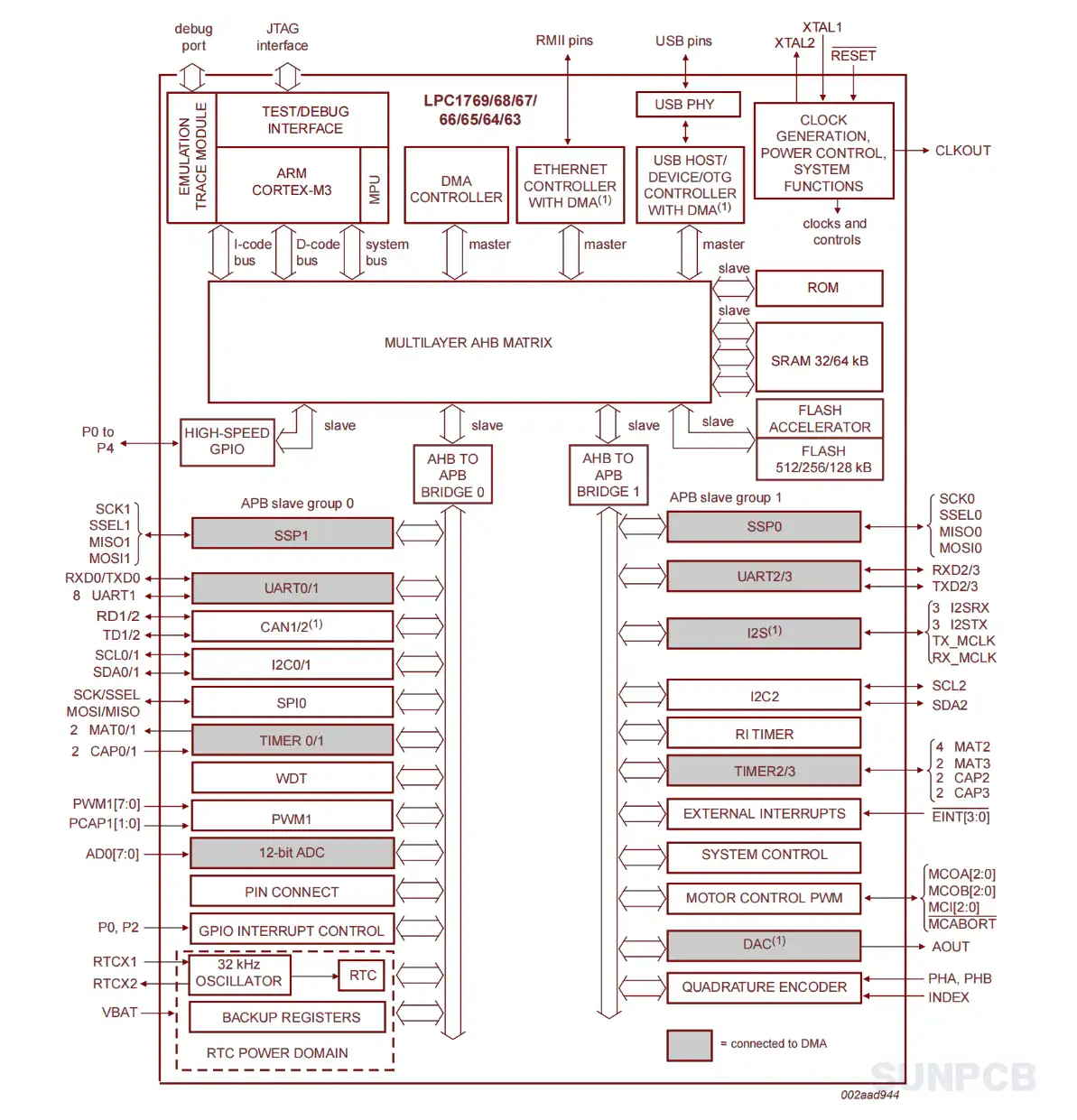
Functional Block Diagram on
![]() LPC1768FBD100 functional block diagram pdf download (P8/P93)
LPC1768FBD100 functional block diagram pdf download (P8/P93)
5. LPC1768FBD100 NXP Overview
5.1 Description
The LPC1768FBD100 is a 32-bit microcontroller based on the ARM Cortex-M3 core, offering high integration and low power consumption for embedded systems.
5.2 Overview
The LPC17xx series features a 100 MHz ARM Cortex-M3 processor with 512 kB flash and 64 kB SRAM, supporting advanced peripherals like Ethernet and USB.
5.3 Features
- ARM Cortex-M3 core
- Up to 120 MHz operation
- Nested Vectored Interrupt Controller for fast deterministic interrupts
- Wake-up Interrupt Controller allows automatic wake from any priority interrupt
- Memory Protection Unit
- Four reduced power modes: Sleep, Deep-sleep, Power-down and Deep power-down
- Memories
- Up to 512 KB Flash memory
- Up to 64 KB SRAM
- Serial Peripherals
- 10/100 Ethernet MAC
- USB 2.0 full-speed device/Host/ OTG controller with on-chip PHY
- Four UARTs with fractional baud rate generation, RS-485. modem control I/O, and IrDA
- Two CAN 2.0B controllers
- Three SSP/SPI controllers
- Three I2 C-bus interfaces with one supporting fast mode plus (1 Mbit/s data rates)
- I2S interface for digital audio
- Analog Peripherals
- 12-bit Analog-to-Digital Converter with eight channels
- 10-bit Digital-to-Analog Converter
- Other Peripherals
- Real-Time Clock operating at < 1 uA
- Eight-channel General-Purpose DMA controller
- Up to 70 General Purpose I/O
- Motor control PWM and Quadrature Encoder Interface to support three-phase motors
- Four 32-bit general-purpose timers/counters
- 4 MHz internal RC oscillator trimmed to 1 % accuracy
- Standard JTAG test/debug interface for compatibility with existing tools
- Four reduced power modes: sleep, deep-sleep, power-down, and deep power-down
- Brownout detect with separate threshold for interrupt and forced reset
- Unique device serial number for identification purposes
- Enhanced flash memory accelerator enables high-speed 120 MHz operations with zero wait states
- In-system programming (ISP) via on-chip boot loader software
- In-application programming (IAP) via on-chip boot loader software
- Eight-channel general-purpose DMA controller
- Split APB bus allows high throughput with few stalls between the CPU and DMA
These features enable robust performance but require careful power management.
5.4 Applications
Industrial control; motor drives; consumer electronics; medical devices.
6. LPC1768FBD100 Package Dimension - LQFP-100
The LPC1768FBD100 pin diagram package details are shown below.
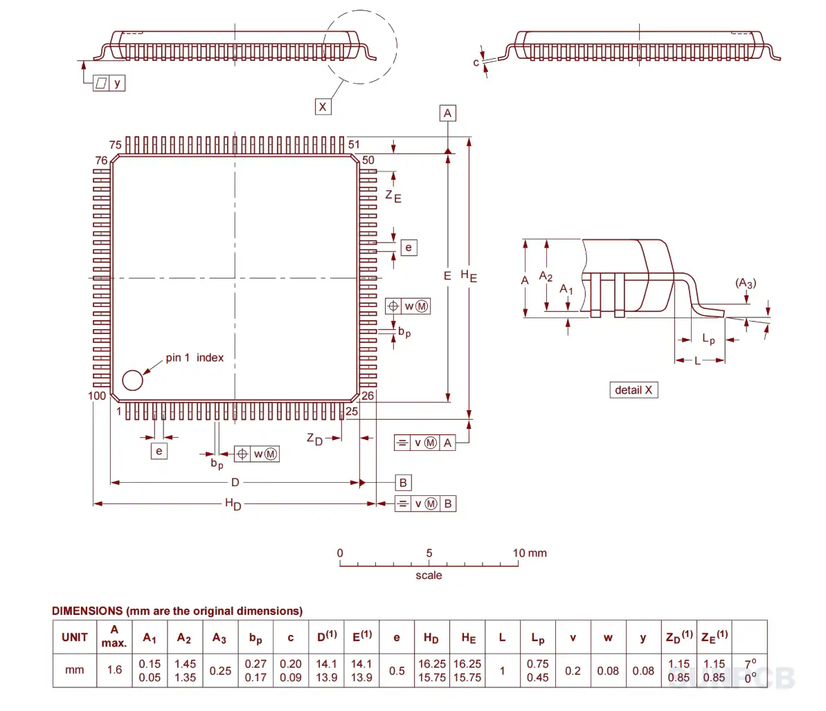
- 14 mm x 14 mm body size.
- 0.5 mm pin pitch.
- 100-pin LQFP package.
7. LPC1768FBD100 FAQs and Tips
Common questions and tips for the LPC1768FBD100 pinout and usage:
- Q: What is the operating voltage?
A: The LPC1768FBD100 operates at 3.3V. - Q: How to configure GPIO pins?
A: Use the PINSEL registers to set pin functions. - Q: Does it support USB?
A: Yes, it includes USB 2.0 Host/Device/OTG. - Q: What is the max clock speed?
A: The core runs at 100 MHz. - Q: Can it handle Ethernet?
A: Yes, it has an Ethernet controller. - Q: How to use the ADC?
A: Configure pins as ADC inputs via PINSEL. - Q: Is there a debug interface?
A: Yes, it supports JTAG and SWD. - Q: What is the flash size?
A: It has 512 kB of flash memory.
Tips:
- Always check pin multiplexing for conflicts.
- Use external pull-up resistors for I2C lines.
- Optimize power consumption in sleep modes.
- Verify clock settings for peripherals.
- Refer to the user manual for register details.