Table of Content
AX31865 Pinout Diagram and Datasheet Overview
This page provides comprehensive information on the MAX31865 RTD-to-Digital Converter, including its pinout diagram, pin configuration, typical application circuits, functional block diagram, and more. Designed for electronic engineers, this resource helps in understanding and integrating the MAX31865 into various projects.
1. MAX31865 Pinout Diagram
The MAX31865 pinout diagram illustrates the pin assignments for both TQFN and SSOP packages.
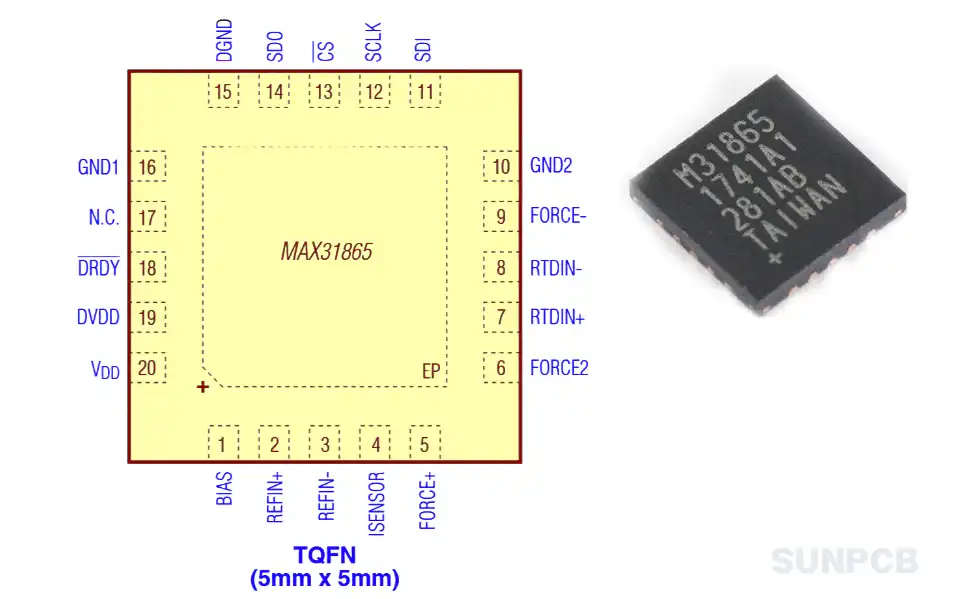
Image: MAX31865 TQFN-20 Pinout Diagram (Page 7/25)
MAX31865 pinout diagram pdf download (P7/P25) ![]()
2. MAX31865 Pin Configuration and Description TQFN-20 Pin Configuration
| Pin # | Pin Name | Pinout Description |
|---|---|---|
| 1 | BIAS | Bias Voltage Output (V_BIAS). |
| 2 | REFIN+ | Positive Reference Voltage Input. Connect to BIAS. Connect reference resistor between REFIN+ and REFIN-. |
| 3 | REFIN- | Negative Reference Voltage Input. Connect reference resistor between REFIN+ and REFIN-. |
| 4 | ISENSOR | Low Side of R_REF. Connect to REFIN-. |
| 5 | FORCE+ | High-Side RTD Drive. Connect to FORCE2 for 3-wire configuration. Protected to ±45V. |
| 6 | FORCE2 | Positive Input for 3-Wire Only. Connect to FORCE+ for 3-wire, ground for 2-wire/4-wire. Protected to ±45V. |
| 7 | RTDIN+ | Positive RTD Input. Protected to ±45V. |
| 8 | RTDIN- | Negative RTD Input. Protected to ±45V. |
| 9 | FORCE- | Low-Side RTD Return. Protected to ±45V. |
| 10 | GND2 | Analog Ground. Connect to GND1. |
| 11 | SDI | Serial-Data Input. |
| 12 | SCLK | Serial-Data Clock Input. |
| 13 | CS | Active-Low Chip Select. Set CS low to enable serial interface. |
| 14 | SDO | Serial-Data Output. |
| 15 | DGND | Digital Ground. |
| 16 | GND1 | Analog Ground. Connect to GND2. |
| 17 | N.C. | Do Not Connect. |
| 18 | DRDY | Active-Low, Push-Pull, Data-Ready Output. Goes low when new conversion result is available. |
| 19 | DVDD | Digital Supply Voltage Input. Connect to 3.3V, bypass to DGND with 0.1μF capacitor. |
| 20 | V_DD | Analog Supply Voltage Input. Connect to 3.3V, bypass to GND1 with 0.1μF capacitor. |
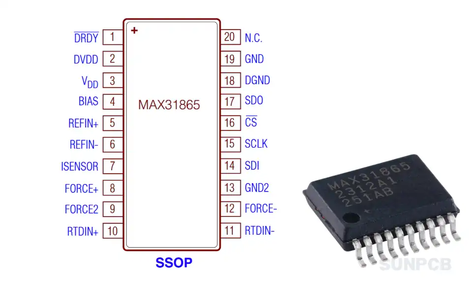
Image: MAX31865 SSOP-20 Pinout Diagram (Page 7/25)
MAX31865 pinout diagram pdf download (P7/P25) ![]()
SSOP-20 Pin Configuration
| Pin # | Pin Name | Pinout Description |
|---|---|---|
| 1 | DRDY | Active-Low, Push-Pull, Data-Ready Output. Goes low when new conversion result is available. |
| 2 | DVDD | Digital Supply Voltage Input. Connect to 3.3V, bypass to DGND with 0.1μF capacitor. |
| 3 | V_DD | Analog Supply Voltage Input. Connect to 3.3V, bypass to GND1 with 0.1μF capacitor. |
| 4 | BIAS | Bias Voltage Output (V_BIAS). |
| 5 | REFIN+ | Positive Reference Voltage Input. Connect to BIAS. Connect reference resistor between REFIN+ and REFIN-. |
| 6 | REFIN- | Negative Reference Voltage Input. Connect reference resistor between REFIN+ and REFIN-. |
| 7 | ISENSOR | Low Side of R_REF. Connect to REFIN-. |
| 8 | FORCE+ | High-Side RTD Drive. Connect to FORCE2 for 3-wire configuration. Protected to ±45V. |
| 9 | FORCE2 | Positive Input for 3-Wire Only. Connect to FORCE+ for 3-wire, ground for 2-wire/4-wire. Protected to ±45V. |
| 10 | RTDIN+ | Positive RTD Input. Protected to ±45V. |
| 11 | RTDIN- | Negative RTD Input. Protected to ±45V. |
| 12 | FORCE- | Low-Side RTD Return. Protected to ±45V. |
| 13 | GND2 | Analog Ground. Connect to GND1. |
| 14 | SDI | Serial-Data Input. |
| 15 | SCLK | Serial-Data Clock Input. |
| 16 | CS | Active-Low Chip Select. Set CS low to enable serial interface. |
| 17 | SDO | Serial-Data Output. |
| 18 | DGND | Digital Ground. |
| 19 | GND1 | Analog Ground. Connect to GND2. |
| 20 | N.C. | Do Not Connect. |
3. MAX31865 Typical Application Circuit Diagram
The typical application circuit diagram illustrates 2-wire, 3-wire, and 4-wire RTD connections for the MAX31865.
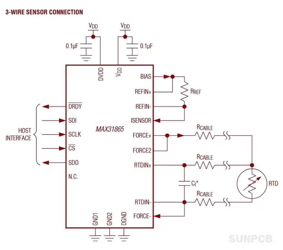
Image: MAX31865 Typical Application Circuit Diagram (Page 24/25)
Summary: The diagram shows configurations for different RTD connections, including recommended external components.
Engineers should note: Select the correct configuration (2-wire, 3-wire, or 4-wire) based on the application. Use 0.1μF bypass capacitors for V_DD and DVDD. For 3-wire setups, connect FORCE+ to FORCE2 to compensate for cable resistance.
4. MAX31865 Functional Block Diagram
The functional block diagram outlines the internal architecture of the MAX31865.
- Power Supplies: V_DD and DVDD power the device.
- V_BIAS Generator: Provides bias voltage for RTD measurements.
- Reference Inputs: REFIN+ and REFIN- set the reference voltage.
- Serial Interface: SPI-compatible interface with SCLK, SDO, SDI, CS.
- 15-Bit ΣΔ ADC: Converts RTD resistance to digital with 0.03125°C resolution.
- ±45V Protection: Protects RTD inputs from overvoltage.
- Fault Detection: Detects open/short conditions in RTD and cables.
- RTD Excitation and Sensing: Provides inputs for 2, 3, or 4-wire RTDs and interfaces with an external reference resistor.
- Precision Delta-Sigma ADC: Converts the ratio of RTD resistance to the reference resistance into a 15-bit digital value.
- SPI-Compatible Interface: Allows communication with a host microcontroller for configuration and data retrieval.
- Fault Detection Logic: Includes programmable detection for open RTD elements, shorted RTDs, and out-of-range voltages.
- Input Protection: Offers robust ±45V protection against overvoltage faults on input pins.
- Voltage Reference Inputs: Fully differential VREF inputs.
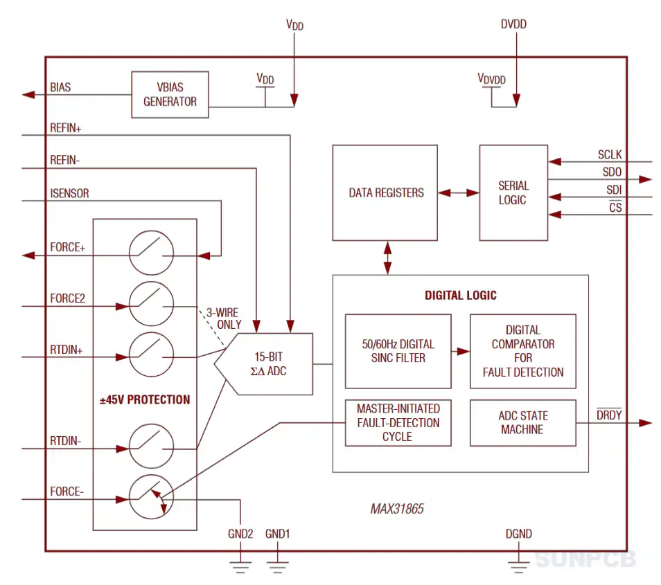
Image: MAX31865 Functional Block Diagram (Page 9/25)
MAX31865 functional block diagram pdf download (P9/P25) ![]()
5. MAX31865 Analog Devices Overview
5.1 Description
The MAX31865 is a resistance-to-digital converter optimized for platinum RTDs. It uses an external reference resistor for sensitivity and a delta-sigma ADC for precise digital conversion. Inputs are protected up to ±45V.
5.2 Overview
The MAX31865 supports 100Ω to 1kΩ RTDs with 2-, 3-, and 4-wire connections. It features a 15-bit ADC, 0.03125°C resolution, and 0.5°C accuracy. The SPI interface ensures easy integration.
5.3 Features
- Simple Conversion of Platinum RTD Resistance to Digital Value
- Handles 100Ω to 1kΩ (at 0°C) Platinum RTDs (PT100 to PT1000)
- Compatible with 2-, 3-, and 4-Wire Sensor Connections
- SPI-Compatible Interface
- Available in 20-Pin TQFN and SSOP Packages
- High Accuracy: 15-Bit ADC Resolution (Nominal 0.03125°C temp. resolution)
- Total Accuracy Over All Operating Conditions: 0.5°C (0.05% of Full Scale) max
- Fully Differential VREF Inputs
- 21ms (max) Conversion Time
- Robust ±45V Input Protection
- Integrated Fault Detection (Open/Short RTD, Out-of-Range Voltage)
Key characteristics: High precision, robust protection, and flexible configurations make the MAX31865 ideal for temperature sensing.
5.4 Applications
Industrial equipment; Medical devices; Instrumentation
6. MAX31865 Parameters
| Specification | Value | Specification | Value |
|---|---|---|---|
| Package Type | 20-pin TQFN, 20-pin SSOP | Supply Voltage (V_DD, DVDD) | 3.0V to 3.6V |
| RTD Resistance Range | 100Ω to 1kΩ | Reference Resistor | 350Ω to 10kΩ |
| ADC Resolution | 15-bit | Temperature Resolution | 0.03125°C |
| Total Accuracy | 0.5°C max | Conversion Time | 21ms max |
| Input Protection | ±45V | Operating Temperature | -40°C to +125°C |
| Standards Compliance | RoHS | Power Consumption | 2mA to 3.5mA (active) |
7. MAX31865 Electrical Characteristics
| Parameter | Min | Typ | Max | Unit |
|---|---|---|---|---|
| Supply Voltage (V_DD, DVDD) | 3.0 | 3.3 | 3.6 | V |
| Power-Supply Current (Active) | 2 | - | 3.5 | mA |
| Shutdown Current | 1.5 | - | 3 | mA |
| ADC Full-Scale Error | -1 | - | 1 | LSB |
| Common-Mode Rejection | - | 90 | - | dB |
| 50/60Hz Noise Rejection | - | 82 | - | dB |
8. MAX31865 Part Numbering System
| Part Number | Package | Temperature Range |
|---|---|---|
| MAX31865ATP+ | 20 TQFN-EP | -40°C to +125°C |
| MAX31865AAP+ | 20 SSOP | -40°C to +125°C |
9. MAX31865 FAQs and Tips
Q: What RTD types are compatible with the MAX31865?
A: The MAX31865 supports 100Ω to 1kΩ platinum RTDs, such as PT100 and PT1000.
Q: How do I select the reference resistor?
A: Use a 400Ω resistor for PT100 and a 4000Ω resistor for PT1000 for optimal sensitivity.
Q: Can I use a 2-wire RTD with the MAX31865?
A: Yes, but 3-wire or 4-wire configurations are preferred for higher accuracy due to cable resistance compensation.
Q: What is the DRDY pin used for?
A: DRDY signals when a new conversion result is available, useful for synchronizing data reads.
Q: How do I protect the MAX31865 from overvoltage?
A: The RTD inputs are protected up to ±45V, but ensure proper grounding and bypass capacitors.
Q: Why is my temperature reading inaccurate?
A: Check the reference resistor value, RTD connection type, and calibration settings.
Q: How fast can the MAX31865 perform conversions?
A: Conversion time is 21ms maximum in continuous mode.
Q: Is the MAX31865 suitable for industrial environments?
A: Yes, its ±45V protection and wide temperature range (-40°C to +125°C) make it ideal for industrial use.
Tips:
- Use a high-precision, low-temperature-coefficient reference resistor (RREF) for best accuracy. Its stability directly impacts measurement accuracy.
- Implement proper PCB layout techniques (see Section 8) to minimize noise coupling, especially around the analog inputs and reference resistor.
- Utilize the fault detection features to enhance system robustness and diagnose connection issues with the RTD sensor.
- For long cable runs, a 4-wire RTD connection is strongly recommended to eliminate errors caused by cable resistance.
- Ensure your microcontroller's SPI communication settings (speed, mode CPOL/CPHA) match the MAX31865 requirements as specified in the datasheet.
- Consider using the built-in mains frequency filter (50Hz/60Hz) in the configuration register to reject noise from power lines, especially in industrial environments.