1. PIC12F1822 Pinout Overview
The PIC12F1822 is an 8-pin, 8-bit microcontroller from Microchip Technology, ideal for compact, low-power applications. This page provides the PIC12F1822 pinout diagram, PIC12F1822 pin configuration, PIC12F1822 pin descripion, schematic, and functional block diagram.
2. PIC12F1822 Pinout Diagram
The PIC12F1822 pinout diagram shows the pin assignments for this 8-pin microcontroller.
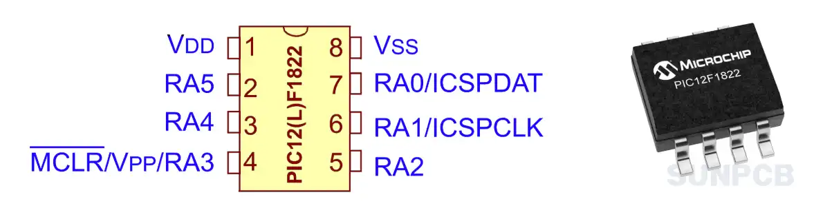
3. PIC12F1822 Pin Configuration and Descripion
The PIC12F1822 pin configuration and PIC12F1822 pin descripion detail each pin's function for the 8pin SOIC, PDIP, and DFN packages.
| Pin# | Pin Name | Type | Pinout Descripion |
|---|---|---|---|
| 1 | VDD | Power | Positive supply voltage (2.3V to 5.5V). |
| 2 | RA5/AN4/OSC1/CLKIN | I/O, Analog, Clock | General-purpose I/O, analog input, external clock input, or oscillator input. |
| 3 | RA4/AN3/OSC2/CLKOUT | I/O, Analog, Clock | General-purpose I/O, analog input, oscillator output, or clock output. |
| 4 | RA3/MCLR/VPP | Input, Reset | Active-low master clear reset or programming voltage input. |
| 5 | RA2/AN2/T0CKI/INT | I/O, Analog, Timer | General-purpose I/O, analog input, Timer0 clock input, or external interrupt. |
| 6 | RA1/AN1/ICSPCLK | I/O, Analog, Program | General-purpose I/O, analog input, or ICSP clock input. |
| 7 | RA0/AN0/ICSPDAT | I/O, Analog, Program | General-purpose I/O, analog input, or ICSP data input/output. |
| 8 | VSS | Power | Ground reference. |
4. PIC12F1822 Typical Application Circuit Diagram
The PIC12F1822 circuit diagram shows a basic setup for using this microcontroller.
Summary: This PIC12F1822 schematic illustrates a minimal circuit with power supply, decoupling capacitors, and MCLR pull-up resistor. Engineers must ensure proper VDD/VSS connections and consider external clock options for precise timing.
5. PIC12F1822 Functional Block Diagram
The PIC12F1822 block diagram outlines the internal architecture of this microcontroller.
- CPU Core: 8-bit PIC architecture with 49 instructions.
- Flash Memory: 3.5 KB program memory, self-reprogrammable.
- Analog Peripherals: 10-bit ADC with 4 channels.
- Timers: One 8-bit and one 16-bit timer.
- Communication: EUSART, MSSP (I2C/SPI) modules.
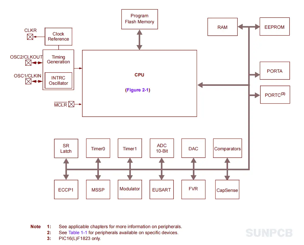
Image: PIC12F1822 Functional Block Diagram
![]() PIC12F1822 functional block diagram pdf download
PIC12F1822 functional block diagram pdf download
6. PIC12F1822 Microchip Overview
6.1 Descripion
The PIC12F1822 is an 8-pin, 8-bit microcontroller from Microchip Technology, designed for low-power, compact applications with enhanced mid-range core.
6.2 Overview
This family of devices contains an enhanced mid-range 8-bit CPU core. The CPU has 49 instructions. Interrupt capability includes automatic context saving. The hardware stack is 16 levels deep and has Overflow and Underflow Reset capability. Direct, Indirect, and Relative Addressing modes are available. Two File Select Registers (FSRs) provide the ability to read program and data memory.
6.3 Features
- Enhanced Mid-Range Core with 49 Instruction, 16 Stack Levels
- Flash Program Memory with self read/write capability
- 128 Bytes of Non-Volatile Data Storage
- Internal 32MHz oscillator
- Power-Saving Sleep mode
- 10-bit ADC, 4 channels
- EUSART for Serial Communications
- MSSP (I2C/SPI)
- ECCP (Enhanced Capture Compare PWM)
Summary: These features make the PIC12F1822 versatile for low-power designs. Engineers should note the limited pin count requires multiplexing functions.
6.4 Applications
Embedded control; Sensor interfacing; Small motor control; Battery-powered devices
7. PIC12F1822 Package Dimension - SOIC-8
The PIC12F1822 pin diagram includes package dimensions for SOIC-8.
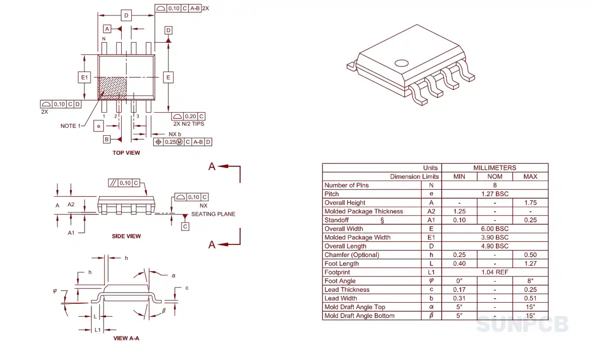
- 8-pin SOIC package, 150 mil body width.
- Pin spacing: 1.27 mm (50 mil).
- Body length: 4.9 mm nominal.
8. PIC12F1822 Layout Example
The datasheet does not provide a specific PIC12F1822 layout example. Check Microchip’s application notes for PCB layout guidelines.
9. PIC12F1822 Part Numbering System
| Part Number | Temperature Range | Package |
|---|---|---|
| PIC12F1822-I/P | -40°C to +85°C | PDIP |
| PIC12F1822-I/SN | -40°C to +85°C | SOIC |
| PIC12F1822-E/MF | -40°C to +125°C | DFN |
10. PIC12F1822 FAQs and Tips
Common questions and tips for using the PIC12F1822 pinout and PIC12F1822 schematic.
Q: What is the operating voltage of PIC12F1822?
A: The PIC12F1822 operates from 2.3V to 5.5V for PIC12F1822, and 1.8V to 3.6V for PIC12LF1822.
Q: How many ADC channels does PIC12F1822 have?
A: It has a 10-bit ADC with 4 channels.
Q: Can PIC12F1822 support I2C and SPI?
A: Yes, it includes an MSSP module for I2C and SPI communication.
Q: What is the MCLR pin used for?
A: The MCLR pin (RA3) is for reset or programming voltage input.
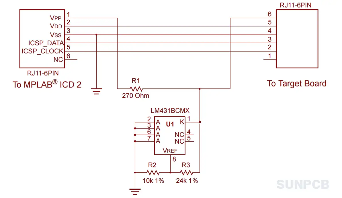
Q: How to program the PIC12F1822?
A: Use ICSP (pins RA0, RA1) with a programmer like PICkit 4.
Q: Is PIC12F1822 suitable for battery-powered devices?
A: Yes, its low-power modes make it ideal for battery applications.
Q: What is the maximum clock frequency?
A: Internal oscillator supports up to 32 MHz.
Q: How to handle unused pins?
A: Configure unused pins as outputs or pull them to VDD/VSS to avoid floating.
Tips for Engineers
- Use decoupling capacitors (0.1 µF) near VDD to stabilize power.
- Enable internal oscillator to reduce external components.
- Check MCLR configuration to avoid unintended resets.
- Leverage EUSART module for serial debugging.
- Optimize ADC settings for low-power applications.