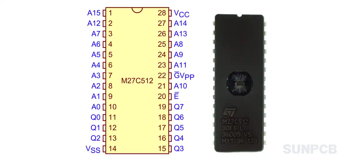
1. M27C512 Pinout Diagram
The M27C512 pinout diagram for the PDIP-28 package is essential for correct wiring. It shows the M27C512 pin configuration clearly.
2. M27C512 Pin Configuration and Description
The M27C512 pin configuration table lists all 28 pins, their names, types, and descriptions. Key pins like VPP, E, and G are bolded for emphasis.
| Pin Number | Pin Name | Description | Pin Number | Pin Name | Description |
|---|---|---|---|---|---|
| 1 | A15 | Address Input [cite: 17, 20] | 28 | VCC | Supply Voltage [cite: 17, 20] |
| 2 | A12 | Address Input [cite: 17, 20] | 27 | A14 | Address Input [cite: 17, 20] |
| 3 | A7 | Address Input [cite: 17, 20] | 26 | A13 | Address Input [cite: 17, 20] |
| 4 | A6 | Address Input [cite: 17, 20] | 25 | A8 | Address Input [cite: 17, 20] |
| 5 | A5 | Address Input [cite: 17, 20] | 24 | A9 | Address Input [cite: 17, 20] |
| 6 | A4 | Address Input [cite: 17, 20] | 23 | A11 | Address Input [cite: 17, 20] |
| 7 | A3 | Address Input [cite: 17, 20] | 22 | GVPP | Output Enable / Program Supply [cite: 17, 20] |
| 8 | A2 | Address Input [cite: 17, 20] | 21 | A10 | Address Input [cite: 17, 20] |
| 9 | A1 | Address Input [cite: 17, 20] | 20 | E | Chip Enable [cite: 17, 20] |
| 10 | A0 | Address Input [cite: 17, 20] | 19 | Q7 | Data Output [cite: 17, 20] |
| 11 | Q0 | Data Output [cite: 17, 20] | 18 | Q6 | Data Output [cite: 17, 20] |
| 12 | Q1 | Data Output [cite: 17, 20] | 17 | Q5 | Data Output [cite: 17, 20] |
| 13 | Q2 | Data Output [cite: 17, 20] | 16 | Q4 | Data Output [cite: 17, 20] |
| 14 | VSS | Ground [cite: 17, 20] | 15 | Q3 | Data Output [cite: 17, 20] |
- E (Chip Enable):
- This is the power control pin and should be used for device selection[cite: 26].
- Applying a CMOS high signal to the E input places the device in standby mode[cite: 29, 31], reducing current consumption and putting outputs in a high impedance state[cite: 30, 31].
- During programming, E is pulsed to VIL (low) while VPP is at 12.75V[cite: 55].
- A high level on E inhibits programming when multiple devices are in parallel[cite: 31, 68].
- GVPP (Output Enable / Program Supply):
- In read mode, this pin functions as Output Enable (G) and should be used to gate data to the output pins[cite: 17, 27].
- During programming, this pin is the program supply voltage (VPP) and requires 12.75V ± 0.25V[cite: 1, 17, 55, 107].
- All inputs are TTL levels except for GVPP (when used as VPP) and 12V on A9 for Electronic Signature[cite: 24].
- VCC must be applied simultaneously with or before VPP and removed simultaneously or after VPP[cite: 101, 104, 107, 109, 114].
- A9 (Address Input):
- For Electronic Signature mode, address line A9 must be raised to 11.5V - 12.5V (typically 12V ± 0.5V)[cite: 33, 73]. All other address lines must be held at VIL during this mode[cite: 74].
- VCC (Supply Voltage):
- The supply voltage for read operation is 5V ± 10%[cite: 1].
- During programming, VCC is specified to be 6.25V ± 0.25V[cite: 57, 107].
- Proper decoupling is crucial. It's recommended to use a 0.1µF ceramic capacitor between VCC and VSS for every device[cite: 43], placed as close as possible to the device[cite: 44].
- Additionally, a 4.7µF bulk electrolytic capacitor should be used between VCC and VSS for every eight devices[cite: 45], located near the power supply connection point[cite: 46].
- Q0-Q7 (Data Outputs/Inputs):
- In read mode, these pins are data outputs[cite: 17, 31].
- During programming, data to be programmed is applied to these pins as inputs[cite: 31, 56].
- System Considerations for Multiple Devices (Two Line Output Control):
- For efficient use, E should be decoded and used as the primary device selecting function[cite: 38].
- G should be made a common connection to all devices in an array and connected to the READ line from the system control bus[cite: 38]. This ensures deselected devices are in low power standby and outputs are active only when data is required[cite: 39].
3. M27C512 Typical Application Circuit Diagram
No typical application circuit diagram is provided in the M27C512 datasheet. For 27C512 programmer schematic or 27C512 eprom programmer circuit, refer to external resources or design your own based on the M27C512 pinout.
4. M27C512 Functional Block Diagram
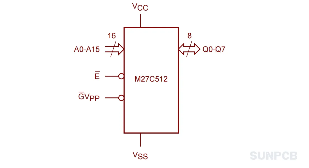
The M27C512 block diagram (Logic Diagram, Figure 1, Page 3) outlines the internal structure. Key points include:
- Address Inputs: A0-A15 for 64K x 8 memory.
- Data Outputs: Q0-Q7 for 8-bit data.
- Control Signals: E and G/VPP manage read and program modes.
- Power Supply: VCC and VSS for operation.
5. M27C512 STMicroelectronics Overview
5.1 Description
The M27C512 is a 512 Kbit UV EPROM and OTP EPROM, organized as 64K x 8. It suits applications needing fast programming.
5.2 Overview
The M27C512 is a 512 Kbit EPROM offered in the two ranges UV (ultra violet erase) and OTP (one time programmable). It is ideally suited for applications where fast turn-around and pattern experimentation are important requirements and is organized as 65536 by 8 bits. The FDIP28W (window ceramic frit-seal package) has transparent lid which allows the user to expose the chip to ultraviolet light to erase the bit pattern. A new pattern can then be written to the device by following the programming procedure. For applications where the content is programmed only one time and erasure is not required, the M27C512 is offered in FDIP28W, PDIP28, and PLCC32 packages. In order to meet environmental requirements, ST offers the M27C512 in ECOPACK packages. ECOPACK packages are Lead-free. The category of second Level Interconnect is marked on the package and on the inner box label, in compliance with JEDEC Standard JESD97. The maximum ratings related to soldering conditions are also marked on the inner box label. ECOPACK is an ST trademark. ECOPACK specifications are available at: www.st.com.
5.3 Features
- 5 V ± 10% supply voltage in read operation
- Access time: 45 ns
- Low power "CMOS" consumption: Active current 30 mA, Standby current 100 µA
- Programming voltage: 12.75 V ± 0.25 V
- Programming time around 6 s
- Electronic Signature: Manufacturer code: 20h, Device code: 3Dh
- Packages: ECOPACK® versions, FDIP28W (F), PDIP28 (B), PLCC32 (C)
These features make the M27C512 ideal for 27C512 programming. Note the UV erasure requirement for FDIP28W packages.
5.4 Applications
Fast turn-around applications; pattern experimentation; one-time programmable systems.
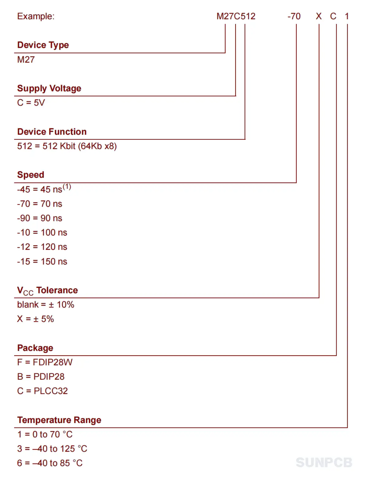
6. M27C512 Part Numbering System
The M27C512 part numbering system is detailed in the Ordering Information Scheme (Table 17, Page 20). It explains the naming conventions.
| Parameter | Option | Description |
|---|---|---|
| Device Type | M27 | EPROM series |
| Supply Voltage | C | 5 V |
| Device Function | 512 | 512 Kbit (64 Kb x 8) |
| Speed | -45, -70, -90, -10, -12, -15 | Access times: 45 ns, 70 ns, 90 ns, 100 ns, 120 ns, 150 ns |
| VCC Tolerance | blank, X | ±10%, ±5% |
| Package | F, B, C | FDIP28W, PDIP28, PLCC32 |
| Temperature Range | 1, 3, 6 | 0 to 70°C, -40 to 125°C, -40 to 85°C |
7. M27C512 FAQs and Tips
FAQs
Q: Can I use a 27C512 programmer for the M27C512?
A: Yes, most universal programmers support the M27C512. I’ve used a 27C512 usb programmer and it works fine if configured for 12.75 V VPP.
Q: How do I erase the M27C512 UV EPROM?
A: Expose the FDIP28W window to 2537 Å UV light for 15-20 minutes. I always cover non-UV areas to prevent damage.
Q: Is there a 27C512 flash replacement?
A: Yes, EEPROMs like the AT28C512 can replace it for non-UV applications. Check pin compatibility first.
Q: What’s the programming voltage for the M27C512?
A: It’s 12.75 V ± 0.25 V. I ensure my 27C512 eprom programmer is calibrated to avoid errors.
Q: Can I read the M27C512 without programming?
A: Yes, set E and G to VIL for read mode. I’ve done this to verify data using a 27C512 eprom read setup.
Q: Is the M27C512 compatible with a 27C512 willem programmer?
A: Yes, Willem programmers support it. Configure for STMicroelectronics settings.
Q: What’s the standby current?
A: It’s 100 µA in CMOS standby mode. I use this to minimize power in low-activity designs.
Q: Is there a 27C512 eeprom equivalent?
A: The AT28C512 is a close match. I’ve swapped it in projects, but verify timing specs.
Tips
- Use a 0.1 µF capacitor between VCC and VSS. I’ve seen noise issues without it in high-speed circuits.
- Apply VCC before VPP. This prevents latch-up, which I’ve encountered in rushed setups.
- Check the UV lamp intensity for erasure. I once used a weak lamp and it took hours.
- Use the PRESTO IIB algorithm for faster programming. It saved me time in prototyping.
- Verify programmed data with tELQV. I caught errors this way in a recent project.
- Label the FDIP28W window to block ambient light. I’ve had accidental erasures in bright labs.