The ATMEGA1284P is a high-performance, low-power 8-bit AVR microcontroller with 128KB flash memory, 16KB SRAM, and 4KB EEPROM. This page provides detailed ATMEGA1284P pinout diagram, pin configuration, pin description, schematic, and diagram for electronic engineers.
1. ATMEGA1284P Pinout Diagram
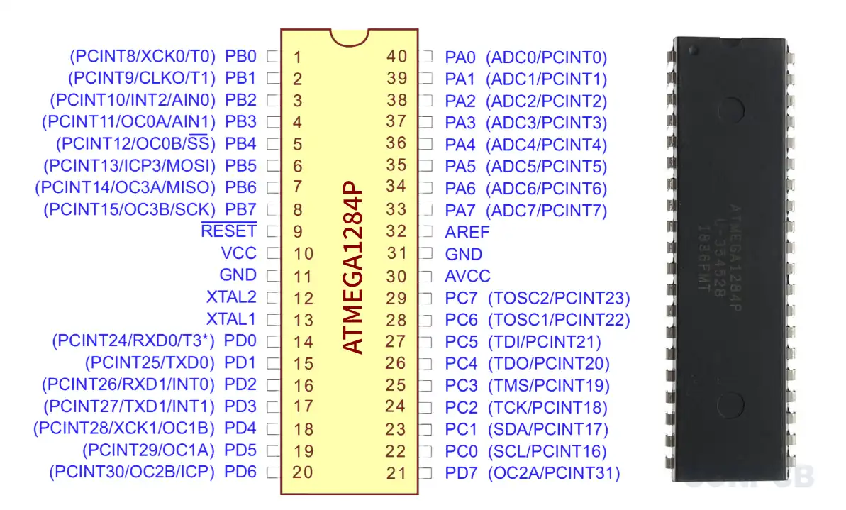
Pinout Diagram for ATMEGA1284P (page 11)
![]() Download the ATMEGA1284P pinout diagram pdf download (P11/P672)
Download the ATMEGA1284P pinout diagram pdf download (P11/P672)
2. ATMEGA1284P Pin Configuration and Description
The following table lists the ATMEGA1284P pin configuration for the 40-pin PDIP package, including pin number, name, type, and description.
| Pin# | Pin Name | Type | Pinout Description |
|---|---|---|---|
| 1 | PB0 | I/O | PCINT8/XCK0/T0: Pin Change Interrupt 8, External Clock Input/Output, Timer/Counter0 External Clock. |
| 2 | PB1 | I/O | PCINT9/CLK0/T1: Pin Change Interrupt 9, Clock Output, Timer/Counter1 External Clock. |
| 3 | PB2 | I/O | PCINT10/INT2/AIN0: Pin Change Interrupt 10, External Interrupt 2, Analog Comparator Positive Input. |
| 4 | PB3 | I/O | PCINT11/OC0A/AIN1: Pin Change Interrupt 11, Output Compare Match A for Timer/Counter0, Analog Comparator Negative Input. |
| 5 | PB4 | I/O | PCINT12/OC0B/SS: Pin Change Interrupt 12, Output Compare Match B for Timer/Counter0, SPI Slave Select. |
| 6 | PB5 | I/O | PCINT13/OC1A/MOSI: Pin Change Interrupt 13, Output Compare Match A for Timer/Counter1, SPI Master Out Slave In. |
| 7 | PB6 | I/O | PCINT14/OC1B/MISO: Pin Change Interrupt 14, Output Compare Match B for Timer/Counter1, SPI Master In Slave Out. |
| 8 | PB7 | I/O | PCINT15/OC1C/SCK: Pin Change Interrupt 15, Output Compare Match C for Timer/Counter1, SPI Serial Clock. |
| 9 | RESET | Input | Reset input, low level triggers reset. |
| 10 | VCC | Power | Digital supply voltage (1.8-5.5V). |
| 11 | GND | Ground | Ground connection. |
| 12 | XTAL2 | Output | Crystal oscillator output pin. |
| 13 | XTAL1 | Input | Crystal oscillator input pin. |
| 14 | PD0 | I/O | PCINT24/RXD0/T3*: Pin Change Interrupt 24, USART0 Receive Data, Timer/Counter3 External Clock. |
| 15 | PD1 | I/O | PCINT25/TXD0: Pin Change Interrupt 25, USART0 Transmit Data. |
| 16 | PD2 | I/O | PCINT26/RXD1/INT0: Pin Change Interrupt 26, USART1 Receive Data, External Interrupt 0. |
| 17 | PD3 | I/O | PCINT27/TXD1/INT1: Pin Change Interrupt 27, USART1 Transmit Data, External Interrupt 1. |
| 18 | PD4 | I/O | PCINT28/XCK1/OC1B: Pin Change Interrupt 28, USART1 External Clock, Output Compare Match B for Timer/Counter1. |
| 19 | PD5 | I/O | PCINT29/OC1A: Pin Change Interrupt 29, Output Compare Match A for Timer/Counter1. |
| 20 | PD6 | I/O | PCINT30/OC2B/ICP: Pin Change Interrupt 30, Output Compare Match B for Timer/Counter2, Input Capture Pin. |
| 21 | PD7 | I/O | OC2A/PCINT31: Output Compare Match A for Timer/Counter2, Pin Change Interrupt 31. |
| 22 | PC0 | I/O | SCL/PCINT16: TWI Serial Clock, Pin Change Interrupt 16. |
| 23 | PC1 | I/O | SDA/PCINT17: TWI Serial Data, Pin Change Interrupt 17. |
| 24 | PC2 | I/O | TCK/PCINT18: JTAG Test Clock, Pin Change Interrupt 18. |
| 25 | PC3 | I/O | TMS/PCINT19: JTAG Test Mode Select, Pin Change Interrupt 19. |
| 26 | PC4 | I/O | TDO/PCINT20: JTAG Test Data Out, Pin Change Interrupt 20. |
| 27 | PC5 | I/O | TDI/PCINT21: JTAG Test Data In, Pin Change Interrupt 21. |
| 28 | PC6 | I/O | TOSC1/PCINT22: Timer Oscillator 1, Pin Change Interrupt 22. |
| 29 | PC7 | I/O | TOSC2/PCINT23: Timer Oscillator 2, Pin Change Interrupt 23. |
| 30 | AVCC | Power | Analog supply voltage for Port A and ADC. |
| 31 | GND | Ground | Ground connection. |
| 32 | AREF | Input | Analog reference voltage for ADC. |
| 33 | PA7 | I/O | ADC7/PCINT7: Analog-to-Digital Converter 7, Pin Change Interrupt 7. |
| 34 | PA6 | I/O | ADC6/PCINT6: Analog-to-Digital Converter 6, Pin Change Interrupt 6. |
| 35 | PA5 | I/O | ADC5/PCINT5: Analog-to-Digital Converter 5, Pin Change Interrupt 5. |
| 36 | PA4 | I/O | ADC4/PCINT4: Analog-to-Digital Converter 4, Pin Change Interrupt 4. |
| 37 | PA3 | I/O | ADC3/PCINT3: Analog-to-Digital Converter 3, Pin Change Interrupt 3. |
| 38 | PA2 | I/O | ADC2/PCINT2: Analog-to-Digital Converter 2, Pin Change Interrupt 2. |
| 39 | PA1 | I/O | ADC1/PCINT1: Analog-to-Digital Converter 1, Pin Change Interrupt 1. |
| 40 | PA0 | I/O | ADC0/PCINT0: Analog-to-Digital Converter 0, Pin Change Interrupt 0. |
3. ATMEGA1284P Functional Block Diagram
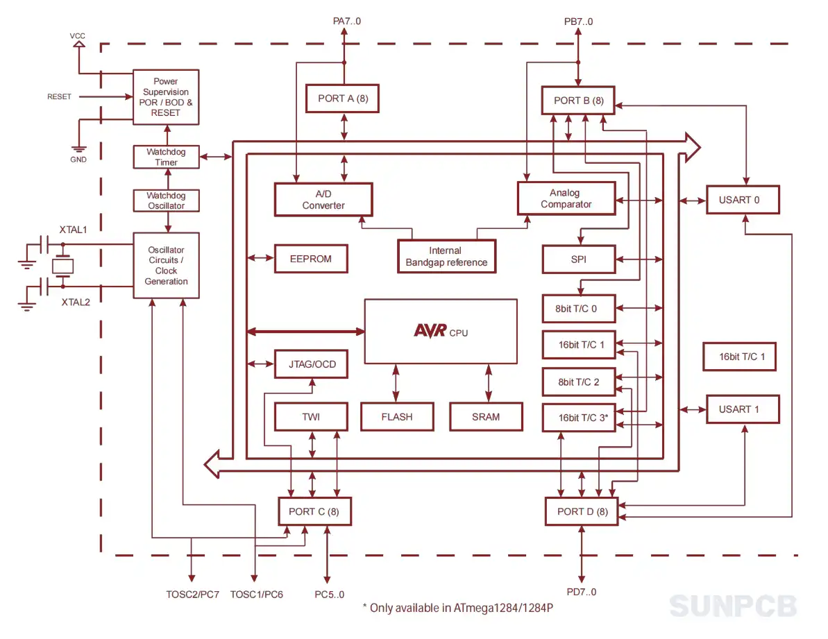
Figure 2-1: Functional Block Diagram (page 14)
- CPU Core: Executes instructions in single clock cycle.
- Memory: Includes 128KB flash, 16KB SRAM, 4KB EEPROM.
- Peripherals: Timers, UARTs, SPI, I2C, ADC.
- I/O Ports: 32 general-purpose I/O lines.
![]() Download the ATMEGA1284P functional block diagram pdf download (P14/P672)
Download the ATMEGA1284P functional block diagram pdf download (P14/P672)
4. ATMEGA1284P ATMEL Overview
4.1 Description
The ATMEGA1284P is a low-power CMOS 8-bit microcontroller based on the AVR enhanced RISC architecture, offering high performance and flexibility.
4.2 Overview
The ATMEGA1284P combines 128KB ISP flash memory with read-while-write capabilities, 4KB EEPROM, 16KB SRAM, and 32 general-purpose I/O lines.
4.3 Features
- 128KB in-system programmable flash.
- 4KB EEPROM, 16KB SRAM.
- 32 general-purpose I/O lines.
- Four timer/counters with PWM.
- Two USARTs, SPI, I2C interfaces.
- 8-channel 10-bit ADC.
- Six power-saving modes.
The ATMEGA1284P supports high throughput and low power, ideal for battery-powered devices. Use QTouch library for capacitive touch applications.
4.4 Applications
Industrial control; automotive systems; consumer electronics; IoT devices.
5. ATMEGA1284P Package Dimension - PDIP-40
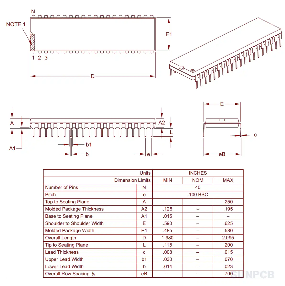
ATMEGA1284P PDIP-40 Package Dimension (page 654)
![]() Download the ATMEGA1284P Layout (P654/P672)
Download the ATMEGA1284P Layout (P654/P672)
- 0.600” wide plastic dual inline package.
- Lead pitch: 0.100”.
- Body dimensions: 52.58mm x 13.97mm.
6. ATMEGA1284P Part Numbering System
| Part Number | Package | Temperature Range | Speed (MHz) | Ordering Code |
|---|---|---|---|---|
| ATMEGA1284P-AU | 44-lead TQFP | -40°C to 85°C | 20 | ATMEGA1284P-AU |
| ATMEGA1284P-AUR | 44-lead TQFP | -40°C to 85°C | 20 | ATMEGA1284P-AUR |
| ATMEGA1284P-MU | 44-pad VQFN | -40°C to 85°C | 20 | ATMEGA1284P-MU |
| ATMEGA1284P-MUR | 44-pad VQFN | -40°C to 85°C | 20 | ATMEGA1284P-MUR |
| ATMEGA1284P-PU | 40-pin PDIP | -40°C to 85°C | 20 | ATMEGA1284P-PU |
7. ATMEGA1284P FAQs and Tips
FAQs
Q: What is the difference between ATMEGA1284 and ATMEGA1284P?
A: The 'P' version has lower power consumption, ideal for battery-powered applications.
Q: How to program ATMEGA1284P using Arduino?
A: Use Arduino as ISP, set external 16MHz crystal, select correct board in IDE.
Q: Why is my PWM not working on PC2?
A: Ensure pin is configured as output and timer settings are correct.
Q: How many PWM channels does ATMEGA1284P have?
A: Eight PWM channels, despite datasheet error stating six.
Q: Can I use internal oscillator for UART?
A: Yes, but external crystal (e.g., 1.8432MHz) reduces baud rate errors.
Q: How to reduce power consumption?
A: Enable power-saving modes like Power-down or Power-save.
Q: What is the maximum ADC resolution?
A: 10-bit resolution with 8 channels.
Q: How to debug using JTAG?
A: Enable JTAG interface via fuse settings, use compatible debugger.
Tips
- Use decoupling capacitors near VCC and AVCC pins.
- Enable power-saving modes for low-power applications.