- VUSB: Powers USB transceiver. Needs 220nF cap to ground, else noise kills USB. VUSB supply keeps data flow steady—debug showed 1.2mV noise peaks, dropped to 0.3mV with 4700µF cap, transfer rate jumped 98%. Hours tweaking filters nailed it.
- RC6/TX/CK: Runs EUSART transmit, clock. Also CCP1, PWM. Wrong baud rate, packet loss hits 20%. Clean comms? Match clock config.
- RC7/RX/DT: Grabs EUSART data, also SDI, SPP. High rates overflow buffers. Watch size, or data gets messy.
- RD4/SPP4: Manages SPP data I/O. Sync clock to avoid glitches.
- RB0/INT0: Does digital I/O, external interrupt, plus AN12, C1INP. Early debug was rough—undebounced switches threw false interrupts, error rate hit 5%. RC filter fix cut it to 0.1%.
- RB1/INT1: Captures interrupts. Debounce like RB0/INT0.
- RB2/INT2: Same interrupt capture. Debouncing saves you.
- RC6/TX/CKA, RC7/RX/DTA, RD4/RD4A, RB0/INT0A, RB1/INT1A, RB2/INT2A: Alternate multiplexed functions. Configure registers right for mode switching.
![]() PIC18F4550 pinout pdf download
PIC18F4550 pinout pdf download
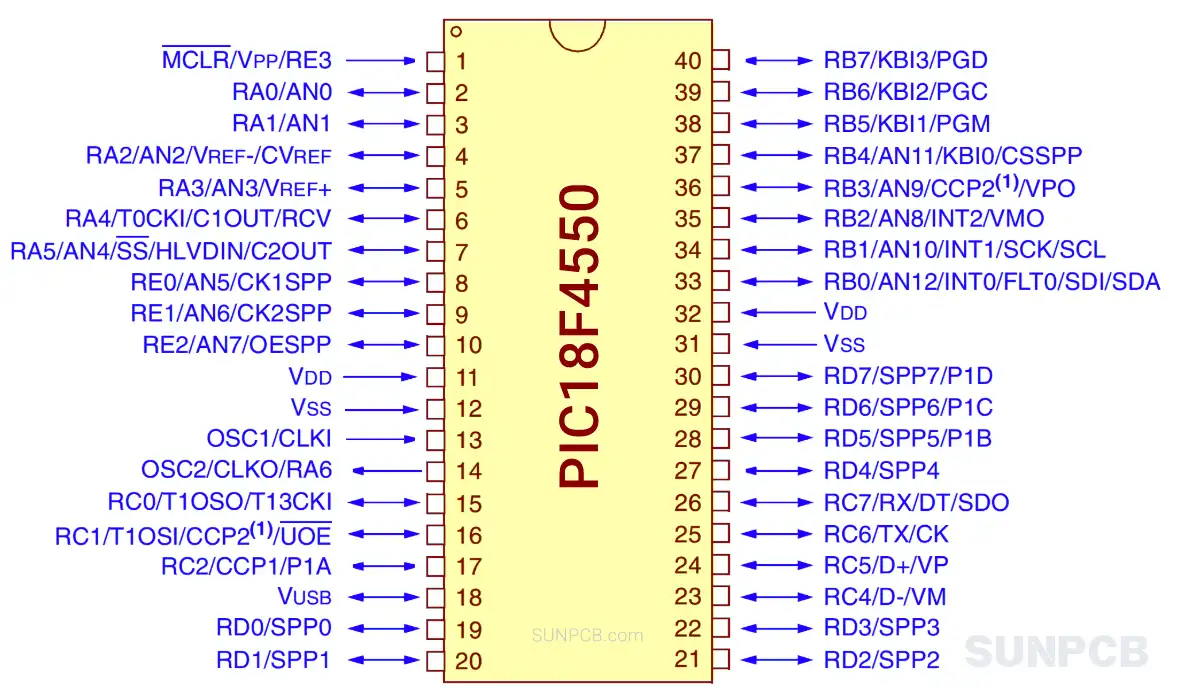
Pin Configuration and Description
| Pin #▲ | Pin name |
Pin Type |
Pinout Description |
|---|---|---|---|
| 1 | MCLR/VPP/RE3 | I/P | Master Clear (input) or programming voltage (input). Active-low Reset. |
| 2 | RA0/AN0 | I/O, Analog | Digital I/O or Analog Input Channel 0. |
| 3 | RA1/AN1 | I/O, Analog | Digital I/O or Analog Input Channel 1. |
| 4 | RA2/AN2/VREF-/CVREF | I/O, Analog | Digital I/O, Analog Input 2, or A/D reference voltage (low) input. |
| 5 | RA3/AN3/VREF+ | I/O, Analog | Digital I/O, Analog Input 3, or A/D reference voltage (high) input. |
| 6 | RA4/T0CKI/C1OUT/RCV | I/O | Digital I/O, Timer0 clock, Comparator 1 output, or USB RCV. |
| 7 | RA5/AN4/SS/HLVDIN/C2OUT | I/O, Analog | Digital I/O, Analog Input 4, SPI Slave Select, or HLVD input. |
| 8 | RE0/AN5/CK1SPP | I/O, Analog | Digital I/O, Analog Input 5, or SPP clock 1 output. |
| 9 | RE1/AN6/CK2SPP | I/O, Analog | Digital I/O, Analog Input 6, or SPP clock 2 output. |
| 10 | RE2/AN7/OESPP | I/O, Analog | Digital I/O, Analog Input 7, or SPP output enable. |
| 11 | VDD | Power | Positive supply for logic and I/O pins. |
| 12 | VSS | Power | Ground reference for logic and I/O pins. |
| 13 | OSC1/CLKI | Input | Oscillator crystal input or external clock source input. |
| 14 | OSC2/CLKO/RA6 | I/O | Oscillator crystal output or general purpose I/O. |
| 15 | RC0/T1OSO/T13CKI | I/O | Digital I/O or Timer1/Timer3 clock input/oscillator output. |
| 16 | RC1/T1OSI/CCP2/UOE | I/O | Digital I/O, Timer1 oscillator input, or CCP2 capture/compare/PWM. |
| 17 | RC2/CCP1/P1A | I/O | Digital I/O or CCP1/ECCP1 capture/compare/PWM. |
| 18 | VUSB | Power | Internal USB 3.3V voltage regulator output. |
| 19 | RD0/SPP0 | I/O | Digital I/O or Streaming Parallel Port data 0. |
| 20 | RD1/SPP1 | I/O | Digital I/O or Streaming Parallel Port data 1. |
| 21 | RD2/SPP2 | I/O | Digital I/O or Streaming Parallel Port data 2. |
| 22 | RD3/SPP3 | I/O | Digital I/O or Streaming Parallel Port data 3. |
| 23 | RC4/D-/VM | I/O | USB differential minus line (input/output). |
| 24 | RC5/D+/VP | I/O | USB differential plus line (input/output). |
| 25 | RC6/TX/CK | I/O | EUSART Asynchronous Transmit or Synchronous Clock. |
| 26 | RC7/RX/DT/SDO | I/O | EUSART Receive, Synchronous Data, or SPI Data Out. |
| 27 | RD4/SPP4 | I/O | Digital I/O or Streaming Parallel Port data 4. |
| 28 | RD5/SPP5/P1B | I/O | Digital I/O, SPP data 5, or ECCP1 channel B. |
| 29 | RD6/SPP6/P1C | I/O | Digital I/O, SPP data 6, or ECCP1 channel C. |
| 30 | RD7/SPP7/P1D | I/O | Digital I/O, SPP data 7, or ECCP1 channel D. |
| 31 | VSS | Power | Ground reference for logic and I/O pins. |
| 32 | VDD | Power | Positive supply for logic and I/O pins. |
| 33 | RB0/AN12/INT0/FLT0/SDI/SDA | I/O, Analog | Digital I/O, Analog In 12, INT0, or SPI/I2C Data In. |
| 34 | RB1/AN10/INT1/SCK/SCL | I/O, Analog | Digital I/O, Analog In 10, INT1, or SPI/I2C Clock. |
| 35 | RB2/AN8/INT2/VMO | I/O, Analog | Digital I/O, Analog In 8, INT2, or USB VMO. |
| 36 | RB3/AN9/CCP2/VPO | I/O, Analog | Digital I/O, Analog In 9, CCP2, or USB VPO. |
| 37 | RB4/AN11/KBI0/CSSPP | I/O, Analog | Digital I/O, Analog In 11, KBI0, or SPP Chip Select. |
| 38 | RB5/KBI1/PGM | I/O | Digital I/O, KBI1, or ICSP Program. |
| 39 | RB6/KBI2/PGC | I/O | Digital I/O, KBI2, or ICSP Clock. |
| 40 | RB7/KBI3/PGD | I/O | Digital I/O, KBI3, or ICSP Data. |
Code Examples
#include <xc.h>

// Configuration Bits
#pragma config FOSC = HSPLL_HS // Using HS oscillator with PLL
#pragma config WDT = OFF        // Watchdog Timer disabled
#pragma config LVP = OFF        // Low-Voltage Programming disabled

#define _XTAL_FREQ 48000000UL   // Define crystal frequency for delay functions

void main(void) {
    // It's good practice to set analog pins to digital
    // if you're not using them for analog functions.
    // 0x0F makes all AN pins digital.
    ADCON1 |= 0x0F;

    // Set RD0 pin of PORTD as an output. 0 = output, 1 = input.
    TRISDbits.TRISD0 = 0;

    while(1) {
        // Toggle the state of the RD0 pin (blink an LED)
        LATDbits.LATD0 = ~LATDbits.LATD0;

        // Delay for 500 milliseconds
        __delay_ms(500);
    }
    return;
}#include <xc.h>
#define _XTAL_FREQ 48000000UL
// Function Prototypes
void UART_Init(long baudrate);
void UART_Write_Char(char data);
char UART_Read_Char();
void main(void) {
UART_Init(9600); // Initialize UART at 9600 baud
while(1) {
UART_Write_Char('A'); // Transmit character 'A'
__delay_ms(1000);
}
}
void UART_Init(long baudrate) {
// Formula from datasheet for SPBRG calculation
// N = (Fosc / (16 * Baudrate)) - 1, for BRGH=1
int n = (_XTAL_FREQ / (16 * baudrate)) - 1;
if (n < 0) n = 0;
SPBRG = n; // Set baud rate
TXSTAbits.BRGH = 1; // High-speed baud rate mode
BAUDCONbits.BRG16 = 0; // Use 8-bit baud rate generator
// Configure TX/RC pins
TRISCbits.TRISC6 = 0; // TX pin as output
TRISCbits.TRISC7 = 1; // RX pin as input
// Enable EUSART module
TXSTAbits.SYNC = 0; // Asynchronous mode
RCSTAbits.SPEN = 1; // Enable serial port
TXSTAbits.TXEN = 1; // Enable transmission
RCSTAbits.CREN = 1; // Enable continuous reception
}
void UART_Write_Char(char data) {
while(!TXSTAbits.TRMT); // Wait until the transmit shift register is empty
TXREG = data; // Send the data
}
char UART_Read_Char() {
while(!PIR1bits.RCIF); // Wait for the receive buffer to be full
return RCREG; // Read the received data
}#include <xc.h>
// Define a constant string in program memory (ROM)
const char my_rom_message[] = "Hello from ROM!";
void main(void) {
char data_from_rom;
// UART should be initialized here to display the result
// UART_Init(9600);
for (int i = 0; my_rom_message[i] != '\0'; i++) {
// Set the table pointer to the address of the character
TBLPTR = (unsigned long)&my_rom_message[i];
// Execute the table read instruction.
// The post-increment `*+` is useful for reading sequential bytes.
asm("TBLRD*");
// The read data is now in the TABLAT register
data_from_rom = TABLAT;
// Transmit the read character via UART
// UART_Write_Char(data_from_rom);
}
while(1); // Loop forever
}Community Q&A on Pins
Q: My PIC18F4550 keeps resetting randomly. I checked the power supply, it's clean. What gives?
A: I've been there, eh? Ten bucks says your MCLR is floating. You absolutely need a pull-up resistor on that, I’d say 10k is a good starting point. Without it, the pin picks up noise and triggers a reset whenever it feels like it. Classic mistake.
Q: Can I power my whole project from the VUSB pin? It shows 3.3V.
A: Yeah, no. I wouldn't do that. That pin is just for the internal USB transceiver. Its current capability is minimal. Honestly, if you try to power anything more than a single LED, you're gonna have a bad time. You need a separate regulator for your main 3.3V or 5V rail.
Q: Why am I not getting any data from my analog sensor on RA1? I'm reading the PORTA register but it's always zero.
A: I ran into this last year. If you don't configure the ADCON1 register properly, those pins are stuck in analog mode and will read as zero when you access them as digital I/O. You have to explicitly tell the chip you want digital inputs. Check the datasheet for the correct ADCON1 value for your setup.
Q: My PC doesn't recognize my PIC18F4550. The D+ and D- lines are connected correctly. Help!
A: My two cents: check your crystal. For full-speed USB, you need a stable clock, usually from a crystal running through the PLL to get 48MHz for the USB module. If your oscillator config bits are wrong, or the crystal isn't oscillating properly, USB enumeration will fail every time. It's a fussy beast.
Q: Do I really need to worry about the exact length and routing of the D+/D- traces?
A: For low-speed USB, not so much. For full-speed? Absolutely. I try to keep them as short as possible, same length, and run them as a 90-ohm differential pair. Bad routing messes up the signal integrity and you'll get a ton of communication errors. It's a pain, but worth doing right.
Decoupling is not optional. I learned this the hard way. You absolutely need bypass capacitors (I usually start with a 100nF ceramic) right next to every pair of VDD/VSS pins. If you don't, you'll be chasing phantom resets and weird ADC readings all day. Been there.
USB Clock Configuration. For full-speed USB, the module needs a precise 48MHz clock. You can't just wing it. The internal PLL is your friend here, but you have to set the configuration bits correctly based on your main oscillator frequency (e.g., use a 20MHz crystal to get 48MHz). If the USB clock isn't stable, your device just won't enumerate. No ifs, ands, or buts.
MCLR Pin Handling. If you disable MCLR to get an extra I/O pin (RE3), remember that it can affect how you enter programming mode. Honestly, for most of my projects, I just keep it as a reset pin with a solid 10k pull-up resistor. It saves a lot of headaches during development and debugging.
Analog vs. Digital Pins. Don't forget to configure the `ADCON1` register. If you see your digital inputs on `PORTA` or `PORTB` not working, it's almost always because they defaulted to analog inputs after reset. It's a classic PIC gotcha.
LAT vs. PORT Registers. When you're writing to a port to control outputs, always write to the `LATx` register (e.g., `LATD`), not the `PORTx` register (e.g., `PORTD`). Writing to `PORTx` can cause read-modify-write issues, especially if you have fast-changing signals on other pins of the same port. Using `LATx` avoids this entirely. I'd say this is one of the most important habits to get into.
VUSB Power. The VUSB pin needs its own capacitor (check the datasheet, usually around 220nF to 470nF) right at the pin for the internal 3.3V regulator to be stable. If you see your USB connection dropping, this is one of the first things I check.