Table of Content
The STM32F411 microcontroller, crafted by STMicroelectronics, is a robust Arm Cortex-M4 MCU. I find its STM32F411 pinout diagram vital for circuit design. The STM32F411 pin configuration supports interfaces like stm32f411 spi and stm32f411 uart, perfect for embedded systems. I share key details below to guide engineers.
1. STM32F411 Pinout Diagram
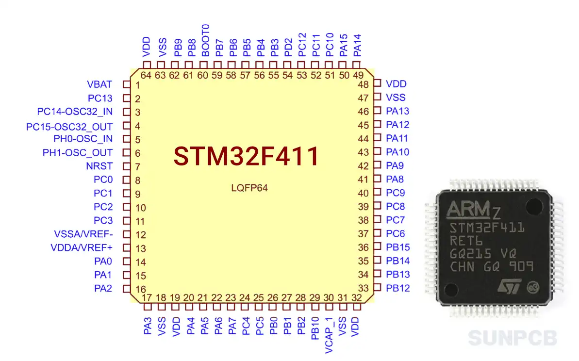
The STM32F411 pinout diagram for LQFP64 shows all 64 pins. It’s essencial for ensuring correct STM32F411 pin configuration for stm32f411 black pill pinout or stm32f411 nucleo pinout.
2. STM32F411 Pin Configuration and Description
The STM32F411 pin configuration table lists all LQFP64 pins. Each pin’s role is detailed for clear STM32F411 pin description. I’ve bolded critical pins for easy reference.
| Pin Number (LQFP64) | Pin Name | Pin Type | I/O Structure | Notes | Alternate Functions | Additional Functions |
|---|---|---|---|---|---|---|
| 1 | VBAT | S | - | - | - | - |
| 2 | PC13-ANTI_TAMP | I/O | FT | (2)(3) | - | RTC_AMP1, RTC_OUT, RTC_TS |
| 3 | PC14-OSC32_IN | I/O | FT | (2)(3)(4) | - | OSC32_IN |
| 4 | PC15-OSC32_OUT | I/O | FT | - | - | OSC32_OUT |
| 5 | PH0 - OSC_IN | I/O | FT | - | - | OSC_IN |
| 6 | PH1 - OSC_OUT | I/O | FT | - | - | OSC_OUT |
| 7 | NRST | I/O | FT | - | EVENTOUT | - |
| 8 | PC0 | I/O | FT | - | EVENTOUT | ADC1_10 |
| 9 | PC1 | I/O | FT | - | EVENTOUT | ADC1_11 |
| 10 | PC2 | I/O | FT | - | SPI2_MISO, I2S2ext_SD, EVENTOUT | ADC1_12 |
| 11 | PC3 | I/O | FT | - | SPI2_MOSI/I2S2_SD, EVENTOUT | ADC1_13 |
| 12 | VSSA/VREF- | S | - | - | - | - |
| 13 | VDDA/VREF+ | S | - | - | - | - |
| 14 | PA0-WKUP | I/O | TC | (5) | TIM2_CH1/TIM2_ET, TIM5_CH1, USART2_CTS, EVENTOUT | ADC1_0, WKUP1 |
| 15 | PA1 | I/O | FT | - | TIM2_CH2, TIM5_CH2, SPI4_MOSI/I2S4_SD, USART2_RTS, EVENTOUT | ADC1_1 |
| 16 | PA2 | I/O | FT | - | TIM2_CH3, TIM5_CH3, TIM9_CH1, I2S2_CKIN, USART2_TX, EVENTOUT | ADC1_2 |
| 17 | PA3 | I/O | FT | - | TIM2_CH4, TIM5_CH4, TIM9_CH2, I2S2_MCK, USART2_RX, EVENTOUT | ADC1_3 |
| 18 | VSS | S | - | - | - | - |
| 19 | VDD | I | FT | - | EVENTOUT | - |
| 20 | PA4 | I/O | FT | - | SPI1_NSS/I2S1_WS, SPI3_NSS/I2S3_WS, USART2_CK, EVENTOUT | ADC1_4 |
| 21 | PA5 | I/O | FT | - | TIM2_CH1/TIM2_ET, SPI1_SCK/I2S1_CK, EVENTOUT | ADC1_5 |
| 22 | PA6 | I/O | FT | - | TIM1_BKIN, TIM3_CH1, SPI1_MISO, I2S2_MCK, SDIO_CMD, EVENTOUT | ADC1_6 |
| 23 | PA7 | I/O | FT | - | TIM1_CH1N, TIM3_CH2, SPI1_MOSI/I2S1_SD, EVENTOUT | ADC1_7 |
| 24 | PC4 | I/O | FT | - | EVENTOUT | ADC1_14 |
| 25 | PC5 | I/O | FT | - | EVENTOUT | ADC1_15 |
| 26 | PB0 | I/O | FT | - | TIM1_CH2N, TIM3_CH3, SPI5_SCK/I2S5_CK, EVENTOUT | ADC1_8 |
| 27 | PB1 | I/O | FT | - | TIM1_CH3N, TIM3_CH4, SPI5_NSS/I2S5_WS, EVENTOUT | ADC1_9 |
| 28 | PB2 | I/O | FT | - | EVENTOUT | BOOT1 |
| 29 | PB10 | I/O | FT | - | TIM2_CH3, I2C2_SCL, SPI2_SCK/I2S2_CK, I2S3_MCK, SDIO_D7, EVENTOUT | - |
| 30 | VCAP_1 | S | - | - | - | - |
| 31 | VSS | S | - | - | - | - |
| 32 | VDD | S | - | - | - | - |
| 33 | PB12 | I/O | FT | - | TIM1_BKIN, I2C2_SMBA, SPI2_NSS/I2S2_WS, SPI4_NSS/I2S4_WS, SPI3_SCK/I2S3_CK, EVENTOUT | - |
| 34 | PB13 | I/O | FT | - | TIM1_CH1N, SPI2_SCK/I2S2_CK, SPI4_SCK/I2S4_CK, EVENTOUT | - |
| 35 | PB14 | I/O | FT | - | TIM1_CH2N, SPI2_MISO, I2S2ext_SD, SDIO_D6, EVENTOUT | - |
| 36 | PB15 | I/O | FT | - | RTC_50Hz, TIM1_CH3N, SPI2_MOSI/I2S2_SD, SDIO_CK, EVENTOUT | RTC_REFIN |
| 37 | PC6 | I/O | FT | - | TIM3_CH1, I2S2_MCK, USART6_TX, SDIO_D6, EVENTOUT | - |
| 38 | PC7 | I/O | FT | - | TIM3_CH2, SPI2_SCK/I2S2_CK, I2S3_MCK, USART6_RX, SDIO_D7, EVENTOUT | - |
| 39 | PC8 | I/O | FT | - | TIM3_CH3, USART6_CK, SDIO_D0, EVENTOUT | - |
| 40 | PC9 | I/O | FT | - | MCO_2, TIM3_CH4, I2C3_SDA, I2S2_CKIN, SDIO_D1, EVENTOUT | - |
| 41 | PA8 | I/O | FT | - | MCO_1, TIM1_CH1, I2C3_SCL, USART1_CK, USB_FS_SOF, SDIO_D1, EVENTOUT | - |
| 42 | PA9 | I/O | FT | - | TIM1_CH2, I2C3_SMBA, USART1_TX, USB_FS_VBUS, SDIO_D2, EVENTOUT | OTG_FS_VBUS |
| 43 | PA10 | I/O | FT | - | TIM1_CH3, SPI5_MOSI/I2S5_SD, USART1_RX, USB_FS_ID, EVENTOUT | - |
| 44 | PA11 | I/O | FT | - | TIM1_CH4, SPI4_MISO, USART1_CTS, USART6_TX, USB_FS_DM, EVENTOUT | - |
| 45 | PA12 | I/O | FT | - | TIM1_ETR, SPI5_MISO, USART1_RTS, USART6_RX, USB_FS_DP, EVENTOUT | - |
| 46 | PA13 | I/O | FT | - | JTMS-SWDIO, EVENTOUT | - |
| 47 | VSS | S | - | - | - | - |
| 48 | VDD | S | - | - | - | - |
| 49 | PA14 | I/O | FT | - | JTCK-SWCLK, EVENTOUT | - |
| 50 | PA15 | I/O | FT | - | JTDI, TIM2_CH1/TIM2_ETR, SPI1_NSS/I2S1_WS, SPI3_NSS/I2S3_WS, USART1_TX, EVENTOUT | - |
| 51 | PC10 | I/O | FT | - | SPI3_SCK/I2S3_CK, SDIO_D2, EVENTOUT | - |
| 52 | PC11 | I/O | FT | - | I2S3ext_SD, SPI3_MISO, SDIO_D3, EVENTOUT | - |
| 53 | PC12 | I/O | FT | - | SPI3_MOSI/I2S3_SD, SDIO_CK, EVENTOUT | - |
| 54 | PD2 | I/O | FT | - | TIM3_ETR, SDIO_CMD, EVENTOUT | - |
| 55 | PB3 | I/O | FT | - | JTDO-SWO, TIM2_CH2, SPI1_SCK/I2S1_CK, SPI3_SCK/I2S3_CK, USART1_RX, I2C2_SDA, EVENTOUT | - |
| 56 | PB4 | I/O | FT | - | JTRST, TIM3_CH1, SPI1_MISO, SPI3_MISO, I2S3ext_SD, I2C3_SDA, SDIO_D0, EVENTOUT | - |
| 57 | PB5 | I/O | TC | - | TIM3_CH2, I2C1_SMBA, SPI1_MOSI/I2S1_SD, SPI3_MOSI/I2S3_SD, SDIO_D3, EVENTOUT | - |
| 58 | PB6 | I/O | FT | - | TIM4_CH1, I2C1_SCL, USART1_TX, EVENTOUT | - |
| 59 | PB7 | I/O | FT | - | TIM4_CH2, I2C1_SDA, USART1_RX, SDIO_D0, EVENTOUT | - |
| 60 | BOOT0 | I | B | - | - | VPP |
| 61 | PB8 | I/O | FT | - | TIM4_CH3, TIM10_CH1, I2C1_SCL, SPI5_MOSI/I2S5_SD, I2C3_SDA, SDIO_D4, EVENTOUT | - |
| 62 | PB9 | I/O | FT | - | TIM4_CH4, TIM11_CH1, I2C1_SDA, SPI2_NSS/I2S2_WS, I2C2_SDA, SDIO_D5, EVENTOUT | - |
| 63 | VSS | S | - | - | - | - |
| 64 | VDD | S | - | - | - | - |
Notes from the datasheet[cite: 1]:
- Function availability depends on the chosen device. [cite: 1]
- PC13, PC14 and PC15 are supplied through the power switch. [cite: 1] Since the switch only sinks a limited amount of current (3 mA), the use of GPIOs PC13 to PC15 in output mode is limited: [cite: 1]
- The speed should not exceed 2 MHz with a maximum load of 30 pF. [cite: 1]
- These I/Os must not be used as a current source (e.g. to drive an LED). [cite: 1]
- Main function after the first backup domain power-up. Later on, it depends on the contents of the RTC registers even after reset (because these registers are not reset by the main reset). [cite: 1] For details on how to manage these I/Os, refer to the RTC register description sections in the STM32F411xx reference manual. [cite: 1]
- FT = 5 V tolerant except when in analog mode or oscillator mode (for PC14, PC15, PH0 and PH1). [cite: 1]
- If the device is delivered in an UFBGA100 and the BYPASS_REG pin is set to VDD (Regulator off/internal reset ON mode), then PA0 is used as an internal Reset (active low). [cite: 1]
![]() STM32F411 pdf download (P15/P151)
STM32F411 pdf download (P15/P151)
Refer to the STM32F411 pinout diagram pdf for full STM32F411 pin description.
3. STM32F411 Typical Application Circuit Diagram
Typical Application Circuit Diagram
The STM32F411 circuit diagram shows USB OTG FS setup. It includes VBUS and ID pin configurations. Engineers must ensure proper external voltage regulator use for VBUS-powered devices and include a current limiter for host mode.
4. STM32F411 Functional Block Diagram
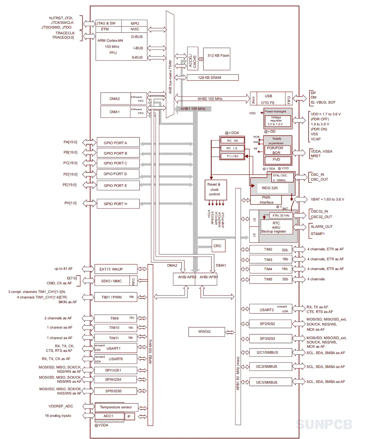
The STM32F411 block diagram highlights core components:
- Cortex-M4: High-performance core with FPU.
- ART Accelerator: Enables fast Flash execution.
- DMA Controller: Supports stm32f411 dma efficiency.
- Timers: 11 timers for stm32f411 timer tasks.
- Communication Interfaces: Includes stm32f411 i2c and stm32f411 usb.
5. STM32F411 STMicroelectronics Overview
5.1 Description
The STM32F411 is a high-efficiency microcontroller with a Cortex-M4 core. It’s optimized for low-power applications.
5.2 Overview
The STM32F411xC/E devices are based on the high-performance Arm Cortex-M4 32-bit RISC core operating at a frequency of up to 100 MHz. The Cortex-M4 core features a Floating point unit (FPU) single precision which supports all Arm single-precision data-processing instructions and data types. It also implements a full set of DSP instructions and a memory protection unit (MPU) which enhances application security.
5.3 Features
- Dynamic Efficiency: Batch acquisition mode (BAM).
- Power Supply: 1.7 V to 3.6 V.
- Core: Arm 32-bit Cortex-M4 CPU with FPU, ART Accelerator, up to 100 MHz, 125 DMIPS.
- Memories: Up to 512 Kbytes Flash, 128 Kbytes SRAM.
- Clock Management: 4-to-26 MHz crystal oscillator, 16 MHz RC, 32 kHz RTC oscillator.
- Power Consumption: Run: 100 µA/MHz; Stop: 9 µA; Standby: 1.8 µA.
- ADC: 1×12-bit, 2.4 MSPS, up to 16 channels.
- DMA: 16-stream DMA with FIFOs.
- Timers: 6×16-bit, 2×32-bit, up to 100 MHz.
- Communication Interfaces: 3×I2C, 3×USARTs, 5×SPI/I2S, SDIO, USB 2.0 FS.
- Other Features: CRC unit, 96-bit unique ID, RTC with subsecond accuracy.
The STM32F411 excels in low-power and high-speed tasks. Pay attention to power supply stability for stm32f411 adc accuracy.
5.4 Applications
Motor drive and application control; Medical equipment; Industrial applications: PLC, inverters, circuit breakers; Printers, and scanners; Alarm systems, video intercom, and HVAC; Home audio appliances; Mobile phone sensor hub.
6. STM32F411 Part Numbering System
The STM32F411 naming rules are listed below, based on the ordering information.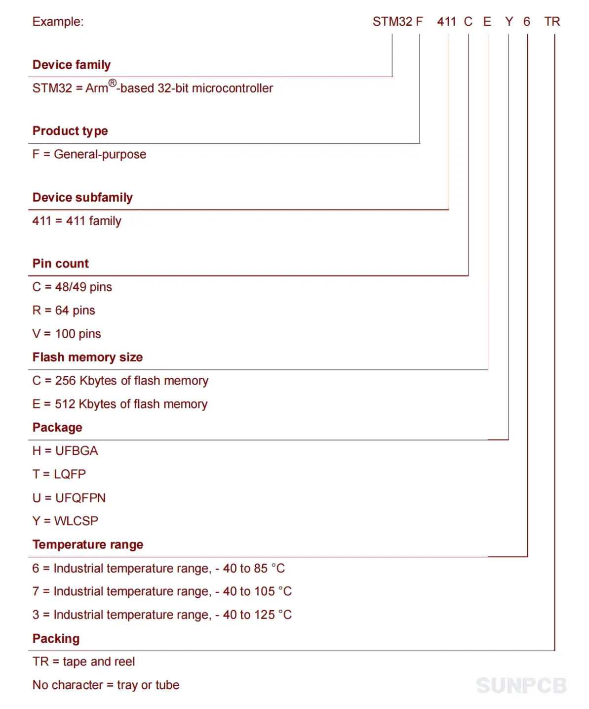
| Reference | Part Number |
|---|---|
| STM32F411xC | STM32F411CC, STM32F411RC, STM32F411VC |
| STM32F411xE | STM32F411CE, STM32F411RE, STM32F411VE |
Bolded part numbers are key variants. Check package and memory sizes in the datasheet.
7. STM32F411 FAQs and Tips
Q: How do I set up STM32F411 UART?
A: I often configure stm32f411 uart. Use PA9 (TX) and PA10 (RX) for USART1. Set alternate function in STM32CubeMX.
Q: Does STM32F411 support USB?
A: Yes, stm32f411 usb is full-speed OTG. Pins PA11 (DM) and PA12 (DP) are used. Add external pull-ups for stability.
Q: How to use STM32F411 ADC effectively?
A: For stm32f411 adc, I recomend using DMA. Pins PA0-PA7 can be ADC inputs. Calibrate to reduce noise.
Q: What’s the best debugging method for STM32F411?
A: Use SWD pins (PA13, PA14). I connect an ST-Link for quick debugging.
Q: Can STM32F411 handle I2C communication?
A: Yes, stm32f411 i2c is reliable. Use PB6 (SCL) and PB7 (SDA) for I2C1. Ensure pull-up resistors.
Q: How to optimize STM32F411 power usage?
A: I use Stop mode to save power. Flash can be powered down for extra savings.
Q: Is STM32F411 good for PWM applications?
A: Absolutely, stm32f411 pwm is versatile. Use TIM1 on PA8 for precise control.
Q: How to interface STM32F411 with SPI devices?
A: For stm32f411 spi, I configure PA5 (SCK), PA6 (MISO), PA7 (MOSI) for SPI1. Check clock polarity.
Tips
- Verify pin multiplexing to avoid conflicts in STM32F411 pin configuration.
- Use external crystal for accurate stm32f411 rtc timing.
- Enable ART Accelerator for faster Flash execution.
- Add pull-up resistors for stm32f411 gpio stability.
- Test DMA channels for stm32f411 dma relibility.