This is MSP430FR5969 pinout and pin configuration for Texas Instruments' ultra-low-power microcontroller. Engineers can find schematics, block diagrams, and the MSP430FR5969 datasheet for design.
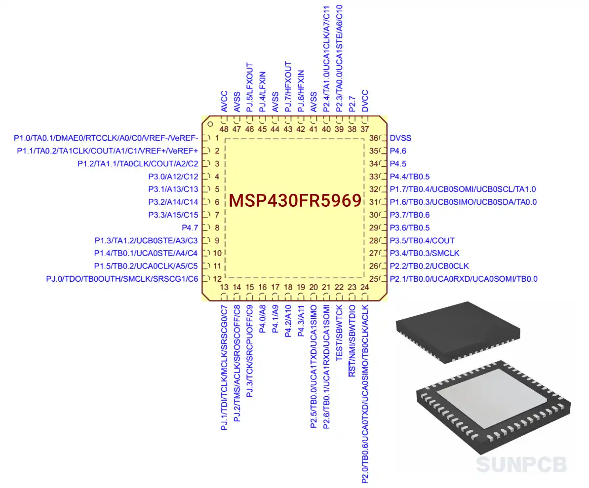
1. MSP430FR5969 Pinout Diagram
The MSP430FR5969 pinout diagram details the 48-pin RGZ package, vital for schematic design.
2. MSP430FR5969 Pin Configuration and Description
This table lists all MSP430FR5969 pins for the 48-pin RGZ package, covering functions like GPIO, ADC, I2C, and UART.
| Pin# | Pin Name | I/O | Pinout Description |
|---|---|---|---|
| 1 | P1.0/TA0.1/DMAE0/RTCCLK/A0/C0/VREF-/VeREF- | I/O | General-purpose digital I/O with port interrupt and wakeup from LPMx.5 TA0 CCR1 capture: CCI1A input, compare: Out1 External DMA trigger RTC clock calibration output (not available on MSP430FR5x5x devices) Analog input A0 for MSP430FR5969 adc12 Comparator input C0 Output of negative reference voltage Input for an external negative reference voltage to the ADC |
| 2 | P1.1/TA0.2/TA1CLK/COUT/A1/C1/VREF+/VeREF+ | I/O | General-purpose digital I/O with port interrupt and wakeup from LPMx.5 TA0 CCR2 capture: CCI2A input, compare: Out2 TA1 input clock Comparator output Analog input A1 for ADC Comparator input C1 Output of positive reference voltage Input for an external positive reference voltage to the ADC |
| 3 | P1.2/TA1.1/TA0CLK/COUT/A2/C2 | I/O | General-purpose digital I/O with port interrupt and wakeup from LPMx.5 TA1 CCR1 capture: CCI1A input, compare: Out1 TA0 input clock Comparator output Analog input A2 for ADC Comparator input C2 |
| 4 | P3.0/A12/C12 | I/O | General-purpose digital I/O with port interrupt and wakeup from LPMx.5 Analog input A12 for ADC Comparator input C12 |
| 5 | P3.1/A13/C13 | I/O | General-purpose digital I/O with port interrupt and wakeup from LPMx.5 Analog input A13 for ADC Comparator input C13 |
| 6 | P3.2/A14/C14 | I/O | General-purpose digital I/O with port interrupt and wakeup from LPMx.5 Analog input A14 for ADC Comparator input C14 |
| 7 | P3.3/A15/C15 | I/O | General-purpose digital I/O with port interrupt and wakeup from LPMx.5 Analog input A15 for ADC Comparator input C15 |
| 8 | P4.7 | I/O | General-purpose digital I/O with MSP430FR5969 pin interrupt and wakeup from LPMx.5 |
| 9 | P1.3/TA1.2/UCB0STE/A3/C3 | I/O | General-purpose digital I/O with port interrupt and wakeup from LPMx.5 TA1 CCR2 capture: CCI2A input, compare: Out2 Slave transmit enable – eUSCI_B0 SPI mode Analog input A3 for ADC Comparator input C3 |
| 10 | P1.4/TB0.1/UCA0STE/A4/C4 | I/O | General-purpose digital I/O with port interrupt and wakeup from LPMx.5 TB0 CCR1 capture: CCI1A input, compare: Out1 Slave transmit enable – eUSCI_A0 SPI mode for MSP430FR5969 spi Analog input A4 for ADC Comparator input C4 |
| 11 | P1.5/TB0.2/UCA0CLK/A5/C5 | I/O | General-purpose digital I/O with port interrupt and wakeup from LPMx.5 TB0 CCR2 capture: CCI2A input, compare: Out2 Clock signal input – eUSCI_A0 SPI slave mode, Clock signal output – eUSCI_A0 SPI master mode Analog input A5 for ADC Comparator input C5 |
| 12 | PJ.0/TDO/TB0OUTH/SMCLK/SRSCG1/C6 | I/O | General-purpose digital I/O Test data output port Switch all PWM outputs high impedance input – TB0 SMCLK output Low-Power Debug: CPU Status Register Bit SCG1 Comparator input C6 |
| 13 | PJ.1/TDI/TCLK/MCLK/SRSCG0/C7 | I/O | General-purpose digital I/O Test data input or test clock input MCLK output Low-Power Debug: CPU Status Register Bit SCG0 Comparator input C7 |
| 14 | PJ.2/TMS/ACLK/SROSCOFF/C8 | I/O | General-purpose digital I/O Test mode select ACLK output Low-Power Debug: CPU Status Register Bit OSCOFF Comparator input C8 |
| 15 | PJ.3/TCK/SRCPUOFF/C9 | I/O | General-purpose digital I/O Test clock Low-Power Debug: CPU Status Register Bit CPUOFF Comparator input C9 |
| 16 | P4.0/A8 | I/O | General-purpose digital I/O with port interrupt and wakeup from LPMx.5 Analog input A8 for ADC |
| 17 | P4.1/A9 | I/O | General-purpose digital I/O with port interrupt and wakeup from LPMx.5 Analog input A9 for ADC |
| 18 | P4.2/A10 | I/O | General-purpose digital I/O with port interrupt and wakeup from LPMx.5 Analog input A10 for ADC |
| 19 | P4.3/A11 | I/O | General-purpose digital I/O with port interrupt and wakeup from LPMx.5 Analog input A11 for ADC |
| 20 | P2.5/TB0.0/UCA1TXD/UCA1SIMO | I/O | General-purpose digital I/O with port interrupt and wakeup from LPMx.5 TB0 CCR0 capture: CCI0B input, compare: Out0 Transmit data – eUSCI_A1 UART mode for MSP430FR5969 uart Slave in, master out – eUSCI_A1 SPI mode |
| 21 | P2.6/TB0.1/UCA1RXD/UCA1SOMI | I/O | General-purpose digital I/O with port interrupt and wakeup from LPMx.5 TB0 CCR1 compare: Out1 Receive data – eUSCI_A1 UART mode Slave out, master in – eUSCI_A1 SPI mode |
| 22 | TEST/SBWTCK | I | Test mode pin – select digital I/O on JTAG pins Spy-Bi-Wire input clock |
| 23 | RST/NMI/SBWTDIO | I/O | Reset input active low Nonmaskable interrupt input Spy-Bi-Wire data input/output |
| 24 | P2.0/TB0.6/UCA0TXD/UCA0SIMO/TB0CLK/ACLK | I/O | General-purpose digital I/O with port interrupt and wakeup from LPMx.5 TB0 CCR6 capture: CCI6B input, compare: Out6 Transmit data – eUSCI_A0 UART mode for MSP430FR5969 uart BSL Transmit (UART BSL) Slave in, master out – eUSCI_A0 SPI mode TB0 clock input ACLK output |
| 25 | P2.1/TB0.0/UCA0RXD/UCA0SOMI/TB0.0 | I/O | General-purpose digital I/O with port interrupt and wakeup from LPMx.5 TB0 CCR0 capture: CCI0A input, compare: Out0 Receive data – eUSCI_A0 UART mode BSL receive (UART BSL) Slave out, master in – eUSCI_A0 SPI mode TB0 CCR0 capture: CCI0A input, compare: Out0 |
| 26 | P2.2/TB0.2/UCB0CLK | I/O | General-purpose digital I/O with port interrupt and wakeup from LPMx.5 TB0 CCR2 compare: Out2 Clock signal input – eUSCI_B0 SPI slave mode Clock signal output – eUSCI_B0 SPI master mode |
| 27 | P3.4/TB0.3/SMCLK | I/O | General-purpose digital I/O with port interrupt and wakeup from LPMx.5 TB0 CCR3 capture: CCI3A input, compare: Out3 SMCLK output |
| 28 | P3.5/TB0.4/COUT | I/O | General-purpose digital I/O with port interrupt and wakeup from LPMx.5 TB0 CCR4 capture: CCI4A input, compare: Out4 Comparator output |
| 29 | P3.6/TB0.5 | I/O | General-purpose digital I/O with port interrupt and wakeup from LPMx.5 TB0 CCR5 capture: CCI5A input, compare: Out5 |
| 30 | P3.7/TB0.6 | I/O | General-purpose digital I/O with port interrupt and wakeup from LPMx.5 TB0 CCR6 capture: CCI6A input, compare: Out6 |
| 31 | P1.6/TB0.3/UCB0SIMO/UCB0SDA/TA0.0 | I/O | General-purpose digital I/O with port interrupt and wakeup from LPMx.5 TB0 CCR3 capture: CCI3B input, compare: Out3 Slave in, master out – eUSCI_B0 SPI mode I2C data – eUSCI_B0 I2C mode for MSP430FR5969 i2c BSL Data (I2C BSL) TA0 CCR0 capture: CCI0A input, compare: Out0 |
| 32 | P1.7/TB0.4/UCB0SOMI/UCB0SCL/TA1.0 | I/O | General-purpose digital I/O with port interrupt and wakeup from LPMx.5 TB0 CCR4 capture: CCI4B input, compare: Out4 Slave out, master in – eUSCI_B0 SPI mode I2C clock – eUSCI_B0 I2C mode BSL clock (I2C BSL) TA1 CCR0 capture: CCI0A input, compare: Out0 |
| 33 | P4.4/TB0.5 | I/O | General-purpose digital I/O with port interrupt and wakeup from LPMx.5 TB0CCR5 capture: CCI5B input, compare: Out5 |
| 34 | P4.5 | I/O | General-purpose digital I/O with port interrupt and wakeup from LPMx.5 |
| 35 | P4.6 | I/O | General-purpose digital I/O with port interrupt and wakeup from LPMx.5 |
| 36 | DVSS | - | Digital ground supply |
| 37 | DVCC | - | Digital power supply |
| 38 | P2.7 | I/O | General-purpose digital I/O with port interrupt and wakeup from LPMx.5 |
| 39 | P2.3/TA0.0/UCA1STE/A6/C10 | I/O | General-purpose digital I/O with port interrupt and wakeup from LPMx.5 TA0 CCR0 capture: CCI0B input, compare: Out0 Slave transmit enable – eUSCI_A1 SPI mode Analog input A6 for ADC Comparator input C10 |
| 40 | P2.4/TA1.0/UCA1CLK/A7/C11 | I/O | General-purpose digital I/O with port interrupt and wakeup from LPMx.5 TA1 CCR0 capture: CCI0B input, compare: Out0 Clock signal input – eUSCI_A1 SPI slave mode Clock signal output – eUSCI_A1 SPI master mode Analog input A7 for ADC Comparator input C11 |
| 41 | AVSS | - | Analog ground supply |
| 42 | PJ.6/HFXIN | I/O | General-purpose digital I/O Input for high-frequency crystal oscillator HFXT (in RHA and DA packages: MSP430FR595x devices only) |
| 43 | PJ.7/HFXOUT | I/O | General-purpose digital I/O Output for high-frequency crystal oscillator HFXT (in RHA and DA packages: MSP430FR595x devices only) |
| 44 | AVSS | - | Analog ground supply |
| 45 | PJ.4/LFXIN | I/O | General-purpose digital I/O Input for low-frequency crystal oscillator LFXT (in RHA and DA packages: MSP430FR594x devices only) |
| 46 | PJ.5/LFXOUT | I/O | General-purpose digital I/O Output of low-frequency crystal oscillator LFXT (in RHA and DA packages: MSP430FR594x devices only) |
| 47 | AVSS | - | Analog ground supply |
| 48 | AVCC | - | Analog power supply |
| Pad | QFN Pad | - | QFN package exposed thermal pad. TI recommends connection to VSS. |
3. MSP430FR5969 Functional Block Diagram
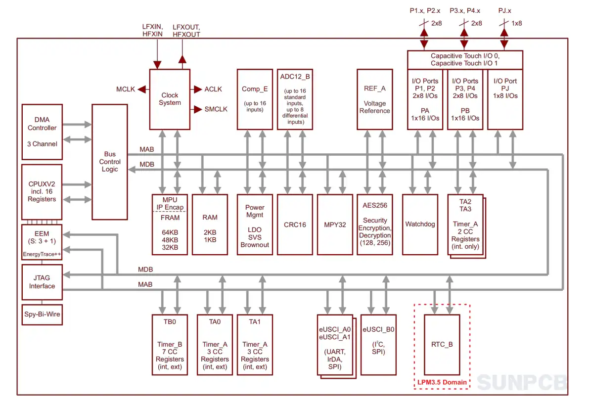
The functional block diagram illustrates the microcontroller's architecture, including MSP430FR5969 fram and peripherals.
- FRAM: Non-volatile memory for data storage.
- CPU: 16-bit MSP430 CPU for processing.
- Peripherals: ADC12_B, timers, and eUSCI modules.
- Clock System: Low- and high-frequency oscillators.
4. MSP430FR5969 Texas Instruments Overview
4.1 Description
The ti MSP430FR5969 is an ultra-low-power microcontroller with FRAM, a 16-bit CPU, and peripherals for efficient designs.
4.2 Overview
The MSP430 ULP portfolio features FRAM, a 16-bit CPU, and intelligent peripherals for various applications. Its seven low-power modes extend battery life.
4.3 Features
- Ultra-low-power FRAM memory
- 16-bit MSP430 CPU
- Seven low-power modes
- ADC12_B with 16 channels
- UART, SPI, and I2C interfaces
- High- and low-frequency oscillators
These features enable power-efficient designs. Configure low-power modes for optimal performance.
4.4 Applications
Sensing; Measurement; Energy harvesting; Wearable devices
5. MSP430FR5969 Package Dimension - VQFN-48
The MSP430FR5969 48 rgz package dimensions are critical for PCB layout design.
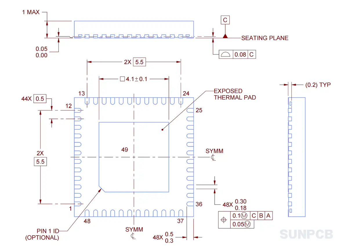
- Dimensions: 7 mm x 7 mm body size.
- Thermal Pad: Connect to VSS for thermal performance.
- Pin Pitch: 0.5 mm for precise soldering.
6. MSP430FR5969 Layout Example
The MSP430FR5969 schematic layout example guides PCB design for the VQFN-48 package.
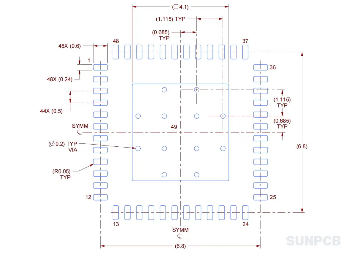
- Thermal Pad: Solder to PCB for heat dissipation.
- Vias: Optional, refer to datasheet.
- Solder Mask: Defined for precise soldering.
7. MSP430FR5969 Part Numbering System
The part numbering system clarifies variants of the MSP430FR5969 package.
| Part Number | FRAM (KB) | SRAM (KB) | Package | I/O Pins |
|---|---|---|---|---|
| MSP430FR5969 | 64 | 2 | VQFN (RGZ) 48 | 40 |
| MSP430FR59691 | 64 | 2 | VQFN (RGZ) 48 | 40 |
| MSP430FR5968 | 48 | 2 | VQFN (RGZ) 48 | 40 |
| MSP430FR5967 | 32 | 1 | VQFN (RGZ) 48 | 40 |
8. MSP430FR5969 FAQs and Tips
Common questions about MSP430FR5969 pins and schematic design, with practical tips.
Q: What is the advantage of MSP430FR5969 FRAM?
A: FRAM offers fast writes and low power compared to flash.
Q: How to configure MSP430FR5969 pin interrupts?
A: Enable interrupts on GPIO pins (e.g., P4.7) via PxIE registers, clear PxIFG to avoid false triggers.
Q: Can UART and I2C BSL be used together?
A: Only one BSL mode (UART on P2.0/P2.1 or I2C on P1.6/P1.7) is supported per device.
Q: What is the MSP430FR5969 ADC12 resolution?
A: ADC12 provides 12-bit resolution with 16 channels, accessible via pins like P1.0.
Q: How to connect unused pins?
A: Tie unused GPIO pins to VSS or VCC via resistors to prevent floating.
Q: How to use MSP430FR5969 crystal pins?
A: Connect 32kHz crystal to LFXIN/LFXOUT (pins 42/41) with 12-18pF capacitors.
Q: Any MSP430FR5969 pin interrupt examples?
A: Configure P1.0 for interrupt with P1IE |= BIT0; clear P1IFG before enabling.
Q: Are there known pin interrupt issues?
A: Some interrupt flags may persist; refer to MSP430FR5969 datasheet errata for details.
Tips:
- Configure low-power modes to save battery life.
- Use FRAM for frequent data logging.
- Connect thermal pad to VSS for heat dissipation.
- Verify BSL pins for bootloader mode.
- Add decoupling capacitors near DVCC/AVCC.