The PCF8574P is an 8-bit I/O expander for I2C-bus, designed by NXP Semiconductors. This page provides the PCF8574P pinout diagram, pin configuration, pin descripton, schematic, and functional block diagram. Ideal for engineers working on microcontroller-based systems.
1. PCF8574P Pinout Diagram
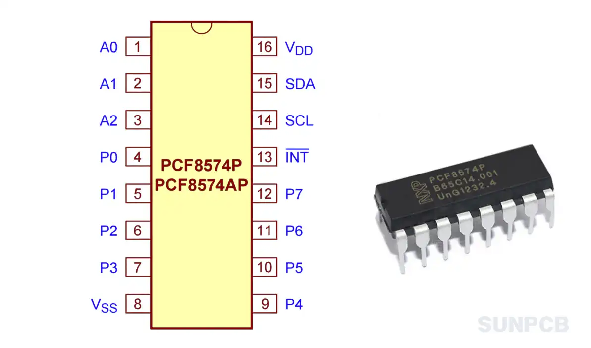
PCF8574P Pinout Diagram
![]() PCF8574P pinout diagram pdf download (P4/P33)
PCF8574P pinout diagram pdf download (P4/P33)
2. PCF8574P Pin Configuration and Descripton
| Pin# | Pin Name | Type | Pinout Descripton |
|---|---|---|---|
| 1 | A0 | Input | Address input 0 for I2C-bus slave address |
| 2 | A1 | Input | Address input 1 for I2C-bus slave address |
| 3 | A2 | Input | Address input 2 for I2C-bus slave address |
| 4 | P0 | I/O | Quasi-bidirectional I/O pin 0 |
| 5 | P1 | I/O | Quasi-bidirectional I/O pin 1 |
| 6 | P2 | I/O | Quasi-bidirectional I/O pin 2 |
| 7 | P3 | I/O | Quasi-bidirectional I/O pin 3 |
| 8 | VSS | Power | Ground (0V) |
| 9 | P4 | I/O | Quasi-bidirectional I/O pin 4 |
| 10 | P5 | I/O | Quasi-bidirectional I/O pin 5 |
| 11 | P6 | I/O | Quasi-bidirectional I/O pin 6 |
| 12 | P7 | I/O | Quasi-bidirectional I/O pin 7 |
| 13 | INT | Output | Interrupt output (active LOW) |
| 14 | SCL | Input | Serial clock line for I2C-bus |
| 15 | SDA | I/O | Serial data line for I2C-bus |
| 16 | VDD | Power | Supply voltage (2.5V to 6V) |
3. PCF8574P Functional Block Diagram
- I2C-bus interface: Handles communication protocol.
- 8-bit I/O port: Quasi-bidirectional pins for input/output.
- Interrupt logic: Generates interrupt signals.
- Address decoder: Sets device slave address.
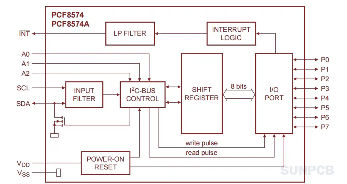
PCF8574P Functional Block Diagram, Page 3
![]() PCF8574P functional block diagram pdf download (P3/P33)
PCF8574P functional block diagram pdf download (P3/P33)
4. PCF8574P NXP Overview
4.1 Descripton
The PCF8574P is a CMOS circuit for I2C-bus applications. It provides remote I/O expansion for microcontrollers. The device features an 8-bit quasi-bidirectional port and low power consumption.
4.2 Overview
The PCF8574 is a silicon CMOS circuit. It provides general purpose remote I/O expansion for most microcontroller families via the two-line bidirectional bus (I2C-bus). The device consists of an 8-bit quasi-bidirectional port and an I2C-bus interface.
4.3 Features
- 8-bit quasi-bidirectional I/O port
- I2C-bus interface with slave address selection
- Low standby current consumption
- Interrupt output for microcontroller notification
- High current drive for direct LED connection
The PCF8574P excels in low-power applications. Ensure proper pull-up resistors on SDA and SCL lines.
4.4 Applications
LED driving; Sensor interfacing; Keypad scanning; General-purpose I/O expansion
5. PCF8574P Package Dimension - DIP-16
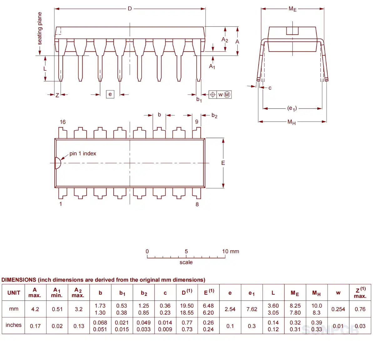
PCF8574P Package Dimension
- 16-pin DIP package
- Standard 300-mil wide body
- Pin spacing: 100 mil
6. PCF8574P Part Numbering System
| Part Number | Package | Descripton |
|---|---|---|
| PCF8574P | DIP-16 | Standard I2C-bus I/O expander |
| PCF8574T | SO-16 | Surface-mount version |
| PCF8574AT | SO-16 | Alternate address version |
7. PCF8574P FAQs and Tips
Q: What is the PCF8574P used for?
A: It expands I/O ports for microcontrollers via I2C-bus.
Q: How many devices can connect to one I2C bus?
A: Up to 8, using address pins A0-A2.
Q: What is the max I2C bus speed?
A: 100 kHz (standard mode).
Q: Can it drive LEDs directly?
A: Yes, with high-current outputs.
Q: Is a pull-up resistor needed?
A: Yes, on SDA and SCL lines.
Q: What is the interrupt pin for?
A: Signals input changes to the microcontroller.
Q: Can it work at 3.3V?
A: Yes, VDD supports 2.5V to 6V.
Q: Is PCF8574P compatible with PCF8574A?
A: Yes, but they have different I2C addresses.
Tips
- Use pull-up resistors (4.7kΩ typical) on I2C lines.
- Connect interrupt pin to microcontroller for efficient polling.
- Check slave address configuration before use.
- Ensure VDD voltage matches system (3.3V or 5V).
- Test I/O pins for sink/source current limits.