The STM32F407 microcontroller, developed by STMicroelectronics, is a powerful Arm Cortex-M4 based MCU. I find its STM32F407 pinout diagram critical for designing reliable circuits. The STM32F407 pin configuration supports multiple interfaces like stm32f407 spi, stm32f407 uart, and stm32f407 usb, making it ideal for complex applications. Below, I share key details to help engineers utilize the STM32F407 effectively.
1. STM32F407 Pinout Diagram
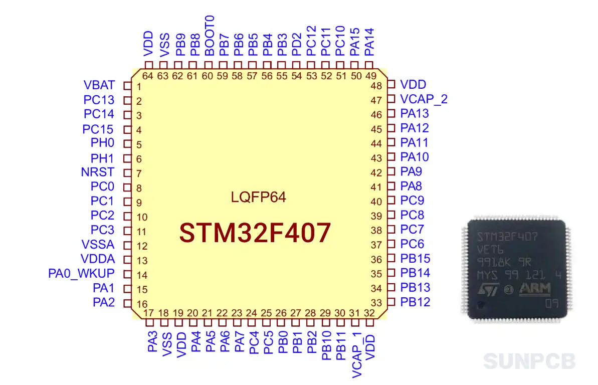
The STM32F407 pinout diagram for the LQFP64 package provides a clear layout of all 64 pins. It’s essencial for engineers to reference this diagram to ensure correct STM32F407 pin configuration for interfaces like stm32f407 can bus or stm32f407 ethernet.
2. STM32F407 Pin Configuration and Description
The STM32F407 pin configuration table below lists all pins for the LQFP64 package. Each pin’s function is detailed to aid in STM32F407 pin description. I’ve highlighted critical pins in bold for quick reference.
| Pin Number | Pin Name | Type | I/O Structure | Notes | Alternate Functions | Additional Functions |
|---|---|---|---|---|---|---|
| 1 | VBAT | S | - | - | - | - |
| 2 | PC13 | I/O | FT | (3)(4) | RTC_OUT, RTC_TAMP1, RTC_TS | - |
| 3 | PC14/OSC32_IN (PC14) | I/O | FT | (3)(4) | - | OSC32_IN(5) |
| 4 | PC15/OSC32_OUT (PC15) | I/O | FT | (3)(4) | - | OSC32_OUT(5) |
| 5 | PH0/OSC_IN (PH0) | I/O | FT | - | EVENTOUT | OSC_IN(5) |
| 6 | PH1/OSC_OUT (PH1) | I/O | FT | - | EVENTOUT | OSC_OUT(5) |
| 7 | NRST | I/O | RST | - | - | - |
| 8 | PC0 | I/O | FT | (5) | OTG_HS_ULPI_STP / EVENTOUT | ADC123_IN10 |
| 9 | PC1 | I/O | FT | (5) | ETH_MDC / EVENTOUT | ADC123_IN11 |
| 10 | PC2 | I/O | FT | (5) | SPI2_MISO / OTG_HS_ULPI_DIR / ETH_MII_TXD2 / I2S2ext_SD / EVENTOUT | ADC123_IN12 |
| 11 | PC3 | I/O | FT | (5) | SPI2_MOSI / I2S2_SD / OTG_HS_ULPI_NXT / ETH_MII_TX_CLK / EVENTOUT | ADC123_IN13 |
| 12 | VSSA | S | - | - | - | - |
| 13 | VDDA | S | - | - | - | - |
| 14 | PA0/WKUP (PA0) | I/O | FT | (6) | USART2_CTS / UART4_TX / ETH_MII_CRS / TIM2_CH1_ETR / TIM5_CH1 / TIM8_ETR / EVENTOUT | ADC123_IN0 / WKUP(5) |
| 15 | PA1 | I/O | FT | (5) | USART2_RTS / UART4_RX / ETH_RMII_REF_CLK / ETH_MII_RX_CLK / TIM5_CH2 / TIM2_CH2 / EVENTOUT | ADC123_IN1 |
| 16 | PA2 | I/O | FT | (5) | USART2_TX / TIM5_CH3 / TIM9_CH1 / TIM2_CH3 / ETH_MDIO / EVENTOUT | ADC123_IN2 |
| 17 | PA3 | I/O | FT | (5) | USART2_RX / TIM5_CH4 / TIM9_CH2 / TIM2_CH4 / OTG_HS_ULPI_D0 / ETH_MII_COL / EVENTOUT | ADC123_IN3 |
| 18 | VSS | S | - | - | - | - |
| 19 | VDD | S | - | - | - | - |
| 20 | PA4 | I/O | TTa | (5) | SPI1_NSS / SPI3_NSS / USART2_CK / DCMI_HSYNC / OTG_HS_SOF / I2S3_WS / EVENTOUT | ADC12_IN4 / DAC_OUT1 |
| 21 | PA5 | I/O | TTa | (5) | SPI1_SCK / OTG_HS_ULPI_CK / TIM2_CH1_ETR / TIM8_CH1N / EVENTOUT | ADC12_IN5 / DAC_OUT2 |
| 22 | PA6 | I/O | FT | (5) | SPI1_MISO / TIM8_BKIN / TIM13_CH1 / DCMI_PIXCLK / TIM3_CH1 / TIM1_BKIN / EVENTOUT | ADC12_IN6 |
| 23 | PA7 | I/O | FT | (5) | SPI1_MOSI / TIM8_CH1N / TIM14_CH1 / TIM3_CH2 / ETH_MII_RX_DV / TIM1_CH1N / ETH_RMII_CRS_DV / EVENTOUT | ADC12_IN7 |
| 24 | PC4 | I/O | FT | (5) | ETH_RMII_RX_D0 / ETH_MII_RX_D0 / EVENTOUT | ADC12_IN14 |
| 25 | PC5 | I/O | FT | (5) | ETH_RMII_RX_D1 / ETH_MII_RX_D1 / EVENTOUT | ADC12_IN15 |
| 26 | PB0 | I/O | FT | (5) | TIM3_CH3 / TIM8_CH2N / OTG_HS_ULPI_D1 / ETH_MII_RXD2 / TIM1_CH2N / EVENTOUT | ADC12_IN8 |
| 27 | PB1 | I/O | FT | (5) | TIM3_CH4 / TIM8_CH3N / OTG_HS_ULPI_D2 / ETH_MII_RXD3 / TIM1_CH3N / EVENTOUT | ADC12_IN9 |
| 28 | PB2/BOOT1 (PB2) | I/O | FT | - | EVENTOUT | - |
| 29 | PB10 | I/O | FT | - | SPI2_SCK / I2S2_CK / I2C2_SCL / USART3_TX / OTG_HS_ULPI_D3 / ETH_MII_RX_ER / TIM2_CH3 / EVENTOUT | - |
| 30 | PB11 | I/O | FT | - | I2C2_SDA / USART3_RX / OTG_HS_ULPI_D4 / ETH_RMII_TX_EN / ETH_MII_TX_EN / TIM2_CH4 / EVENTOUT | - |
| 31 | VCAP_1 | S | - | - | - | - |
| 32 | VDD | S | - | - | - | - |
| 33 | PB12 | I/O | FT | - | SPI2_NSS / I2S2_WS / I2C2_SMBA / USART3_CK / TIM1_BKIN / CAN2_RX / OTG_HS_ULPI_D5 / ETH_RMII_TXD0 / ETH_MII_TXD0 / OTG_HS_ID / EVENTOUT | - |
| 34 | PB13 | I/O | FT | - | SPI2_SCK / I2S2_CK / USART3_CTS / TIM1_CH1N / CAN2_TX / OTG_HS_ULPI_D6 / ETH_RMII_TXD1 / ETH_MII_TXD1 / EVENTOUT | OTG_HS_VBUS |
| 35 | PB14 | I/O | FT | - | SPI2_MISO / TIM1_CH2N / TIM12_CH1 / OTG_HS_DM / USART3_RTS / TIM8_CH2N / I2S2ext_SD / EVENTOUT | - |
| 36 | PB15 | I/O | FT | - | SPI2_MOSI / I2S2_SD / TIM1_CH3N / TIM8_CH3N / TIM12_CH2 / OTG_HS_DP / EVENTOUT | RTC_REFIN |
| 37 | PC6 | I/O | FT | - | I2S2_MCK / TIM8_CH1 / SDIO_D6 / USART6_TX / DCMI_D0 / TIM3_CH1 / EVENTOUT | - |
| 38 | PC7 | I/O | FT | - | I2S3_MCK / TIM8_CH2 / SDIO_D7 / USART6_RX / DCMI_D1 / TIM3_CH2 / EVENTOUT | - |
| 39 | PC8 | I/O | FT | - | TIM8_CH3 / SDIO_D0 / TIM3_CH3 / USART6_CK / DCMI_D2 / EVENTOUT | - |
| 40 | PC9 | I/O | FT | - | I2S_CKIN / MCO2 / TIM8_CH4 / SDIO_D1 / I2C3_SDA / DCMI_D3 / TIM3_CH4 / EVENTOUT | - |
| 41 | PA8 | I/O | FT | - | MCO1 / USART1_CK / TIM1_CH1 / I2C3_SCL / OTG_FS_SOF / EVENTOUT | - |
| 42 | PA9 | I/O | FT | - | USART1_TX / TIM1_CH2 / I2C3_SMBA / DCMI_D0 / EVENTOUT | OTG_FS_VBUS |
| 43 | PA10 | I/O | FT | - | USART1_RX / TIM1_CH3 / OTG_FS_ID / DCMI_D1 / EVENTOUT | - |
| 44 | PA11 | I/O | FT | - | USART1_CTS / CAN1_RX / TIM1_CH4 / OTG_FS_DM / EVENTOUT | - |
| 45 | PA12 | I/O | FT | - | USART1_RTS / CAN1_TX / TIM1_ETR / OTG_FS_DP / EVENTOUT | - |
| 46 | PA13 (JTMS-SWDIO) | I/O | FT | - | JTMS-SWDIO / EVENTOUT | - |
| 47 | VCAP_2 | S | - | - | - | - |
| 48 | VDD | S | - | - | - | - |
| 49 | PA14 (JTCK-SWCLK) | I/O | FT | - | JTCK-SWCLK / EVENTOUT | - |
| 50 | PA15 (JTDI) | I/O | FT | - | JTDI / SPI3_NSS / I2S3_WS / TIM2_CH1_ETR / SPI1_NSS / EVENTOUT | - |
| 51 | PC10 | I/O | FT | - | SPI3_SCK / I2S3_CK / UART4_TX / SDIO_D2 / DCMI_D8 / USART3_TX / EVENTOUT | - |
| 52 | PC11 | I/O | FT | - | UART4_RX / SPI3_MISO / SDIO_D3 / DCMI_D4 / USART3_RX / I2S3ext_SD / EVENTOUT | - |
| 53 | PC12 | I/O | FT | - | UART5_TX / SDIO_CK / DCMI_D9 / SPI3_MOSI / I2S3_SD / USART3_CK / EVENTOUT | - |
| 54 | PD2 | I/O | FT | - | TIM3_ETR / UART5_RX / SDIO_CMD / DCMI_D11 / EVENTOUT | - |
| 55 | PB3 (JTDO/TRACESWO) | I/O | FT | - | JTDO / TRACESWO / SPI3_SCK / I2S3_CK / TIM2_CH2 / SPI1_SCK / EVENTOUT | - |
| 56 | PB4 (NJTRST) | I/O | FT | - | NJTRST / SPI3_MISO / TIM3_CH1 / SPI1_MISO / I2S3ext_SD / EVENTOUT | - |
| 57 | PB5 | I/O | FT | - | I2C1_SMBA / CAN2_RX / OTG_HS_ULPI_D7 / ETH_PPS_OUT / TIM3_CH2 / SPI1_MOSI / SPI3_MOSI / DCMI_D10 / I2S3_SD / EVENTOUT | - |
| 58 | PB6 | I/O | FT | - | I2C1_SCL / TIM4_CH1 / CAN2_TX / DCMI_D5 / USART1_TX / EVENTOUT | - |
| 59 | PB7 | I/O | FT | - | I2C1_SDA / FSMC_NL / DCMI_VSYNC / USART1_RX / TIM4_CH2 / EVENTOUT | - |
| 60 | BOOT0 | I | B | - | - | VPP |
| 61 | PB8 | I/O | FT | - | TIM4_CH3 / SDIO_D4 / TIM10_CH1 / DCMI_D6 / ETH_MII_TXD3 / I2C1_SCL / CAN1_RX / EVENTOUT | - |
| 62 | PB9 | I/O | FT | - | SPI2_NSS / I2S2_WS / TIM4_CH4 / TIM11_CH1 / SDIO_D5 / DCMI_D7 / I2C1_SDA / CAN1_TX / EVENTOUT | - |
| 63 | VSS | S | - | - | - | - |
| 64 | VDD | S | - | - | - | - |
Notes from Datasheet Table 7:
- (3) PC13, PC14, PC15 and PI8 are supplied through the power switch. Since the switch only sinks a limited amount of current (3 mA), the use of GPIOs PC13 to PC15 and PI8 in output mode is limited: The speed should not exceed 2 MHz with a maximum load of 30 pF. These I/Os must not be used as a current source (e.g. to drive an LED). [cite: 523, 524]
- (4) Main function after the first backup domain power-up. Later on, it depends on the contents of the RTC registers even after reset (because these registers are not reset by the main reset). For details on how to manage these I/Os, refer to the RTC register description sections in the STM32F4xx reference manual. [cite: 525, 526]
- (5) FT = 5 V tolerant except when in analog mode or oscillator mode (for PC14, PC15, PH0 and PH1). [cite: 527]
- (6) If the device is delivered in an UFBGA176 or WLCSP90 and the BYPASS_REG pin is set to VDD (Regulator off/internal reset ON mode), then PA0 is used as an internal Reset (active low). [cite: 528] (Note: This specific condition might be less relevant for LQFP64 but is listed for PA0).
Note: The table is abbreviated for brevity. Refer to the STM32F407 pinout diagram pdf for the complete STM32F407 pin description.
3. STM32F407 Typical Application Circuit Diagram
No typical application circuit diagram is provided in the datasheet. Engineers should refer to STMicroelectronics’ application notes for STM32F407 schematic examples, especially for stm32f407 adc or stm32f407 dac setups.
4. STM32F407 Functional Block Diagram
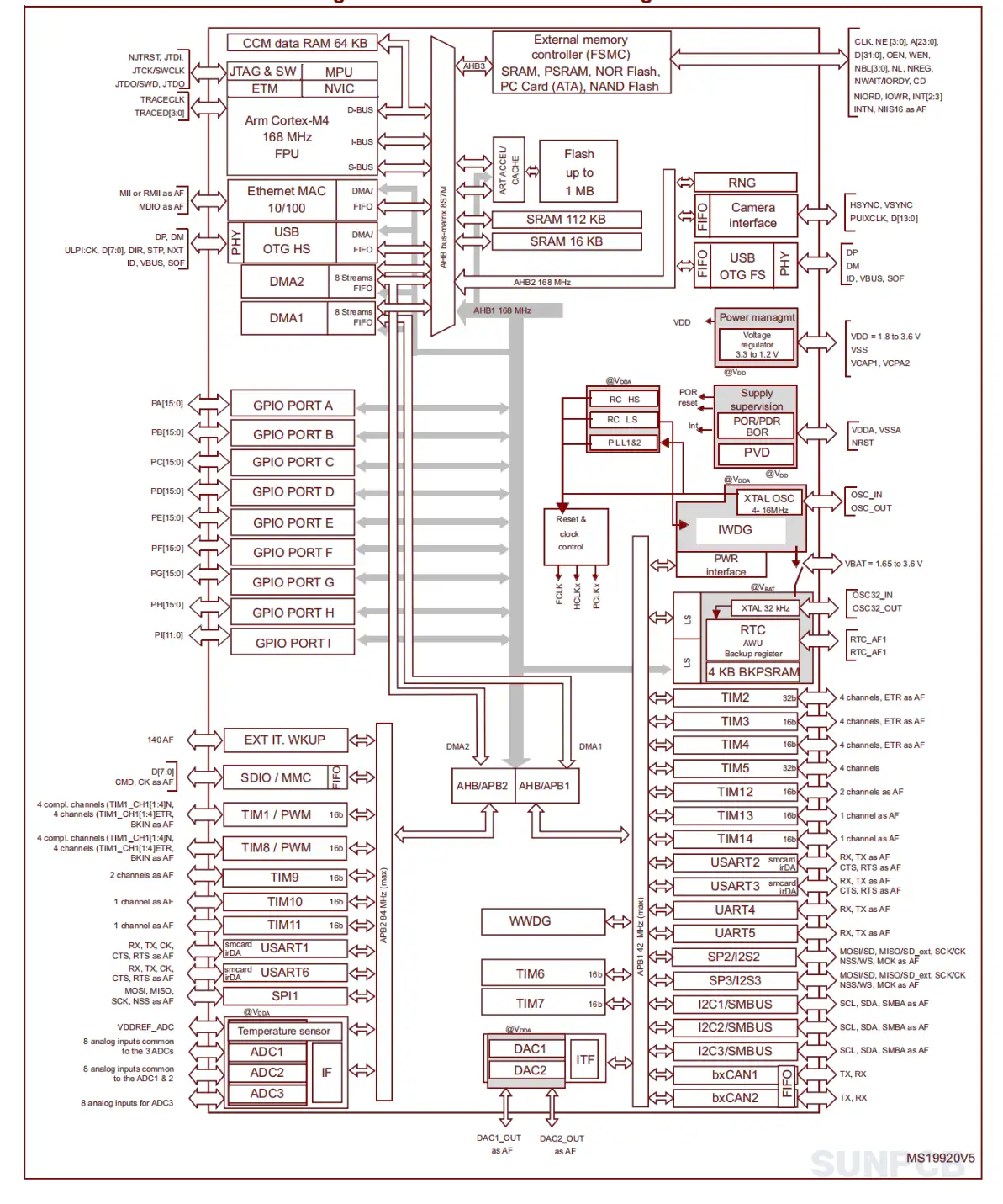
The STM32F407 block diagram outlines the MCU’s architecture. Key points include:
- Arm Cortex-M4: Core with FPU for high-performance processing.
- ART Accelerator: Enables zero-wait state Flash execution.
- DMA Controller: Supports efficient data transfers for stm32f407 dma.
- Communication Interfaces: Includes stm32f407 spi, stm32f407 can, and stm32f407 ethernet.
- Timers: Up to 17 timers for stm32f407 timer applications.
5. STM32F407 STMicroelectronics Overview
5.1 Description
The STM32F407 is a high-performance microcontroller with a Cortex-M4 core. It supports advanced communication interfaces and is suited for demanding applications.
5.2 Overview
The STM32F405xx and STM32F407xx family is based on the high-performance Arm Cortex-M4 32-bit RISC core operating at a frequency of up to 168 MHz. The Cortex-M4 core features a Floating point unit (FPU) single precision which supports all Arm single-precision data-processing instructions and data types. It also implements a full set of DSP instructions and a memory protection unit (MPU) which enhances application security.
5.3 Features
- Core: Arm 32-bit Cortex-M4 CPU with FPU, Adaptive real-time accelerator (ART Accelerator) allowing 0-wait state execution from Flash memory, frequency up to 168 MHz, memory protection unit, 210 DMIPS/1.25 DMIPS/MHz (Dhrystone 2.1), and DSP instructions.
- Memories: Up to 1 Mbyte of Flash memory, Up to 192+4 Kbytes of SRAM including 64-Kbyte of CCM data RAM, 512 bytes of OTP memory, Flexible static memory controller supporting Compact Flash, SRAM, PSRAM, NOR, and NAND memories.
- Clock, Reset, and Supply Management: 1.8 V to 3.6 V application supply and I/Os, POR, PDR, PVD, and BOR, 4-to-26 MHz crystal oscillator, Internal 16 MHz factory-trimmed RC, 32 kHz oscillator for RTC with calibration.
- Low-Power Operation: Sleep, Stop, and Standby modes, VBAT supply for RTC, 20×32-bit backup registers + optional 4 KB backup SRAM.
- ADCs and DACs: 3×12-bit, 2.4 MSPS A/D converters, 2×12-bit D/A converters.
- DMA: 16-stream DMA controller with FIFOs and burst support.
- Timers: Up to 17 timers, including twelve 16-bit and two 32-bit timers up to 168 MHz.
- Communication Interfaces: 3×I2C, 4×USARTs/2×UARTs, 3×SPIs, 2×CAN interfaces, SDIO interface.
- Advanced Connectivity: USB 2.0 FS/HS, 10/100 Ethernet MAC, 8- to 14-bit parallel camera interface.
- Other Features: True random number generator, CRC calculation unit, 96-bit unique ID, RTC with subsecond accuracy.
These features make the STM32F407 versatile for stm32f407 lcd, stm32f407 sd card, and stm32f407 rtc applications. Ensure proper power supply and clock configuration for optimal performance.
5.4 Applications
Motor drive and application control; Medical equipment; Industrial applications: PLC, inverters, circuit breakers; Printers, and scanners; Alarm systems, video intercom, and HVAC; Home audio appliances.
6. STM32F407 Part Numbering System
The STM32F407 part numbering is detailed in the ordering information section. Below is the naming convention.
| Reference | Part Number |
|---|---|
| STM32F407xx | STM32F407VG, STM32F407IG, STM32F407ZG, STM32F407VE, STM32F407ZE, STM32F407IE |
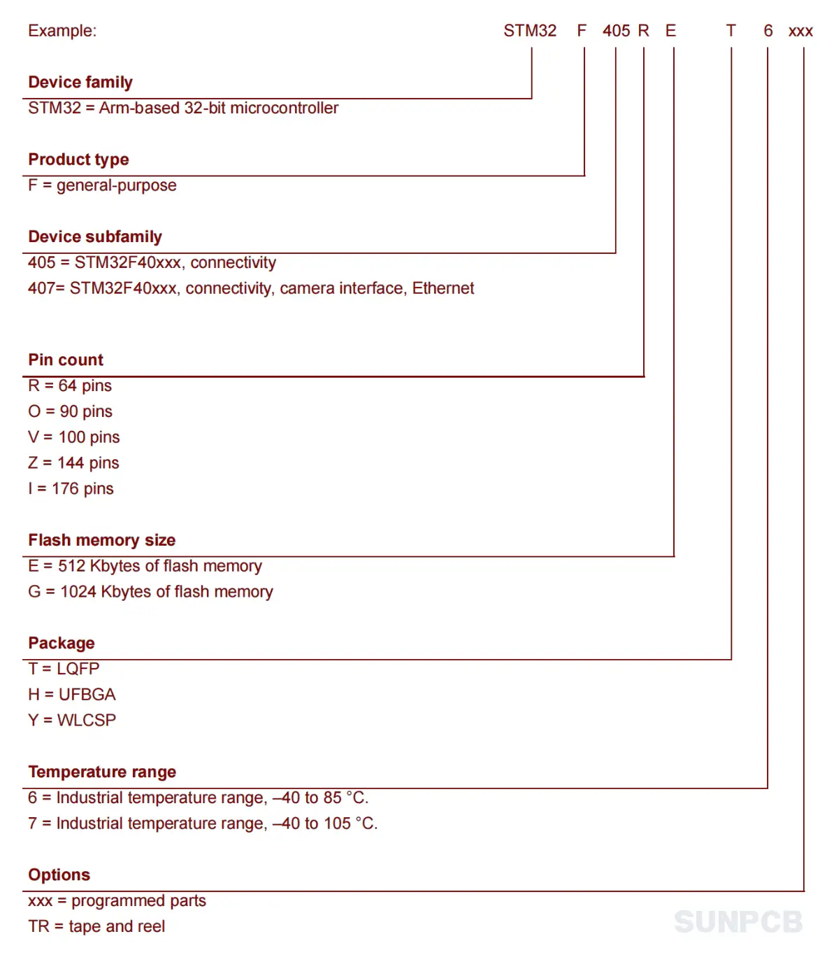
The bolded part numbers indicate common variants. Check the datasheet for package and memory differences.
7. STM32F407 FAQs and Tips
Q: How do I configure the STM32F407 pinout for UART?
A: I often get asked about stm32f407 uart setup. Select pins like PA9 (TX) and PA10 (RX) for USART1. Configure them as alternate function push-pull in your code.
Q: Can STM32F407 support Ethernet?
A: Yes, the stm32f407 ethernet MAC supports 10/100 Mbps. Use pins like PA1, PA2 for RMII. Ensure proper PHY chip integration.
Q: What’s the best way to use STM32F407 ADC?
A: For stm32f407 adc, I recommend using DMA for efficient sampling. Pins like PA0-PA7 can be ADC inputs. Calibrate for accuracy.
Q: How to debug STM32F407 effectively?
A: Use JTAG/SWD pins (PA13, PA14). I connect a debugger like ST-Link to trace issues quickly.
Q: Is STM32F407 suitable for CAN bus?
A: Absolutely, stm32f407 can bus is robust. Use PB8 (CAN1_RX) and PB9 (CAN1_TX). Add a transceiver for reliability.
Q: How to optimize STM32F407 power consumption?
A: Enable low-power modes like Stop or Standby. I adjust the clock frequency to balance performance and power.
Q: Can STM32F407 interface with an SD card?
A: Yes, via stm32f407 sd card SDIO interface. Pins like PC8-PC12 are used. Ensure proper pull-ups.
Q: How to use STM32F407 timers?
A: stm32f407 timer pins like PA8 (TIM1_CH1) are versatile. Configure for PWM or capture modes based on your needs.
Tips
- Always check pin multiplexing to avoid conflicts in STM32F407 pin configuration.
- Use external oscillators for precise stm32f407 rtc timing.
- Enable ART Accelerator to boost Flash execution speed.
- Protect GPIO pins with resistors in stm32f407 gpio designs.
- Test DMA channels thoroughly for stm32f407 dma reliability.