This is a detailed information on the TPA3116 pinout diagram, TPA3116 pin configuration, and TPA3116 pin description. Engineers can find schematics, functional block diagrams, and layout examples for the Texas Instruments TPA3116 Class-D amplifier.
1. TPA3116 Pinout Diagram
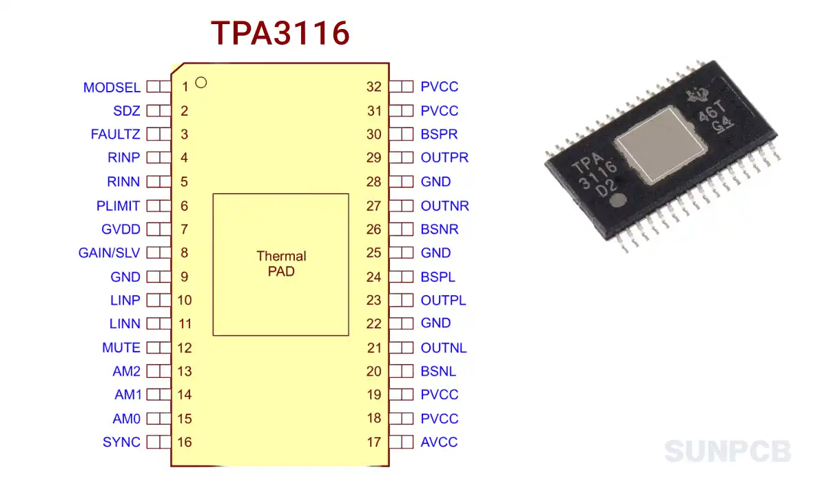
TPA3116 Pinout Diagram (Page 3/49)
![]() TPA3116 pinout diagram pdf download (P3/P49)
TPA3116 pinout diagram pdf download (P3/P49)
2. TPA3116 Pin Configuration and Description
| Pin# | Pin Name | Type | Pinout Description |
|---|---|---|---|
| 1 | MODSEL | I | Mode selection logic input (LOW = BD mode, HIGH = 1 SPW mode). TTL logic levels with compliance to AVCC. |
| 2 | SDZ | I | Shutdown logic input for audio amp (LOW = outputs Hi-Z, HIGH = outputs enabled). TTL logic levels with compliance to AVCC. |
| 3 | FAULTZ | DO | General fault reporting including Over-temp, DC Detect. Open drain. FAULTZ = High, normal operation; FAULTZ = Low, fault condition. |
| 4 | RINP | I | Positive audio input for right channel. Biased at 3 V. |
| 5 | RINN | I | Negative audio input for right channel. Biased at 3 V. |
| 6 | PLIMIT | I | Power limit level adjust. Connect a resistor divider from GVDD to GND to set power limit. Connect directly to GVDD for no power limit. |
| 7 | GVDD | PO | Internally generated gate voltage supply. Connect to 1 µF X7R ceramic decoupling capacitor only. |
| 8 | GAIN/SLV | I | Selects gain and Master/Slave mode via voltage divider. |
| 9 | GND | G | Ground. |
| 10 | LINP | I | Positive audio input for left channel. Biased at 3 V. Connect to GND for PBTL mode. |
| 11 | LINN | I | Negative audio input for left channel. Biased at 3 V. Connect to GND for PBTL mode. |
| 12 | MUTE | I | Mute signal for fast disable/enable of outputs (HIGH = outputs Hi-Z, LOW = outputs enabled). TTL logic levels with compliance to AVCC. |
| 13 | AM2 | I | AM Avoidance Frequency Selection. |
| 14 | AM1 | I | AM Avoidance Frequency Selection. |
| 15 | AMO | I | AM Avoidance Frequency Selection. |
| 16 | SYNC | DIO | Clock input/output for synchronizing multiple class-D devices. Direction set by GAIN/SLV. |
| 17 | AVCC | P | Analog Supply. |
| 18 | PVCC | P | Power supply. |
| 19 | PVCC | P | Power supply. |
| 20 | BSNL | BST | Bootstrap for negative left channel output. Connect to 220 nF X5R capacitor to OUTNL. |
| 21 | OUTNL | PO | Negative left channel output. |
| 22 | GND | G | Ground. |
| 23 | OUTPL | PO | Positive left channel output. |
| 24 | BSPL | BST | Bootstrap for positive left channel output. Connect to 220 nF X5R capacitor to OUTPL. |
| 25 | GND | G | Ground. |
| 26 | BSNR | BST | Bootstrap for negative right channel output. Connect to 220 nF X5R capacitor to OUTNR. |
| 27 | OUTNR | PO | Negative right channel output. |
| 28 | GND | G | Ground. |
| 29 | OUTPR | PO | Positive right channel output. |
| 30 | BSPR | BST | Bootstrap for positive right channel output. Connect to 220 nF X5R capacitor to OUTPR. |
| 31 | PVCC | P | Power supply. |
| 32 | PVCC | P | Power supply. |
| 33 | PowerPAD | G | A: Connect to GND for best system performance. If not connected to GND, leave floating. |
3. TPA3116 Typical Application Circuit Diagram
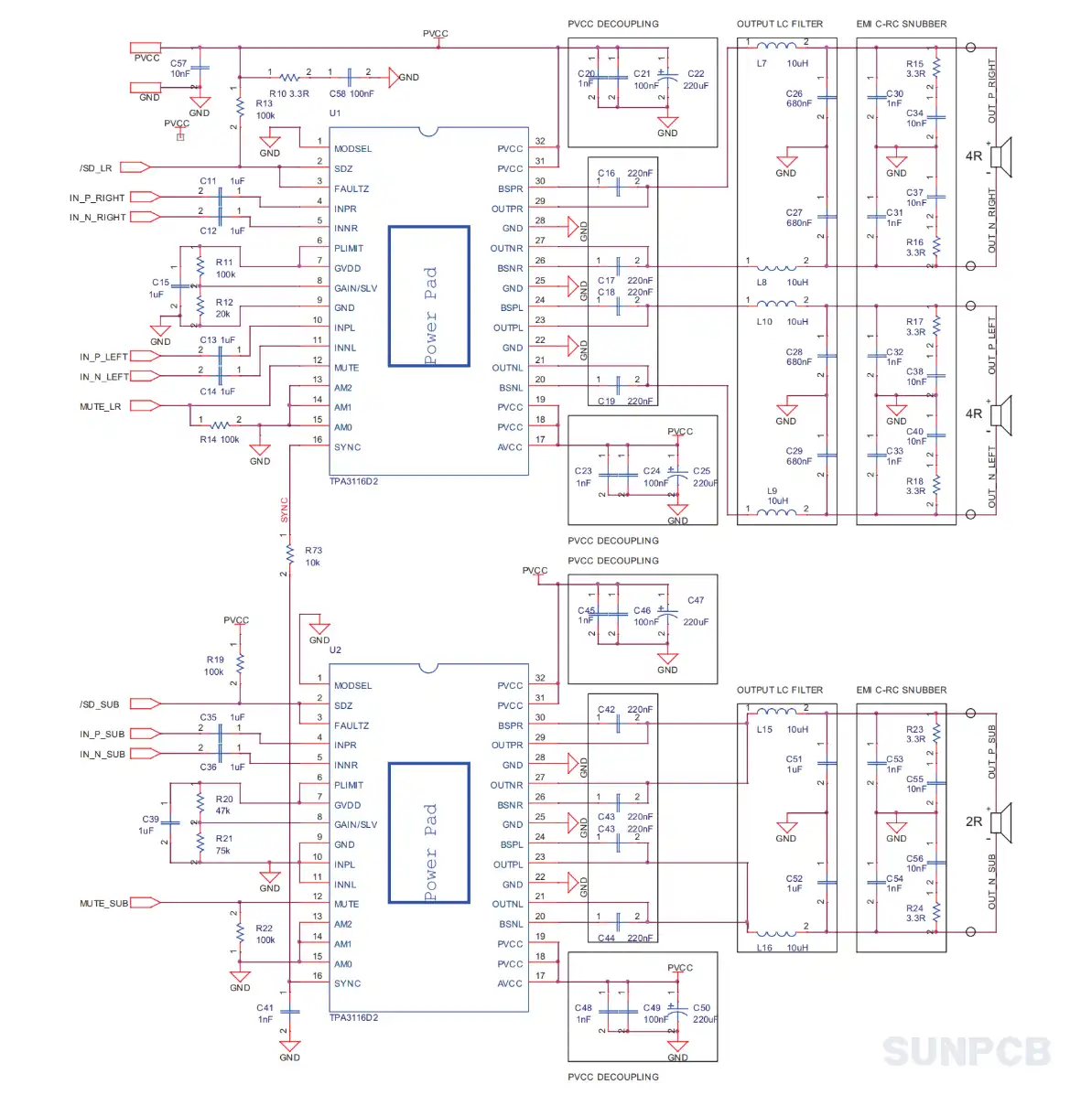
Typical Application Circuit Diagram
![]() TPA3116 circuit diagram pdf download (P26/P49)
TPA3116 circuit diagram pdf download (P26/P49)
The TPA3116 schematic shows a stereo BTL configuration. It includes differential inputs, output filters, and bootstrap capacitors. Engineers must ensure proper decoupling capacitors and grounding for optimal performance. Use 220 nF X5R capacitors for bootstrap pins and a 1 µF X7R capacitor for GVDD.
4. TPA3116 Functional Block Diagram
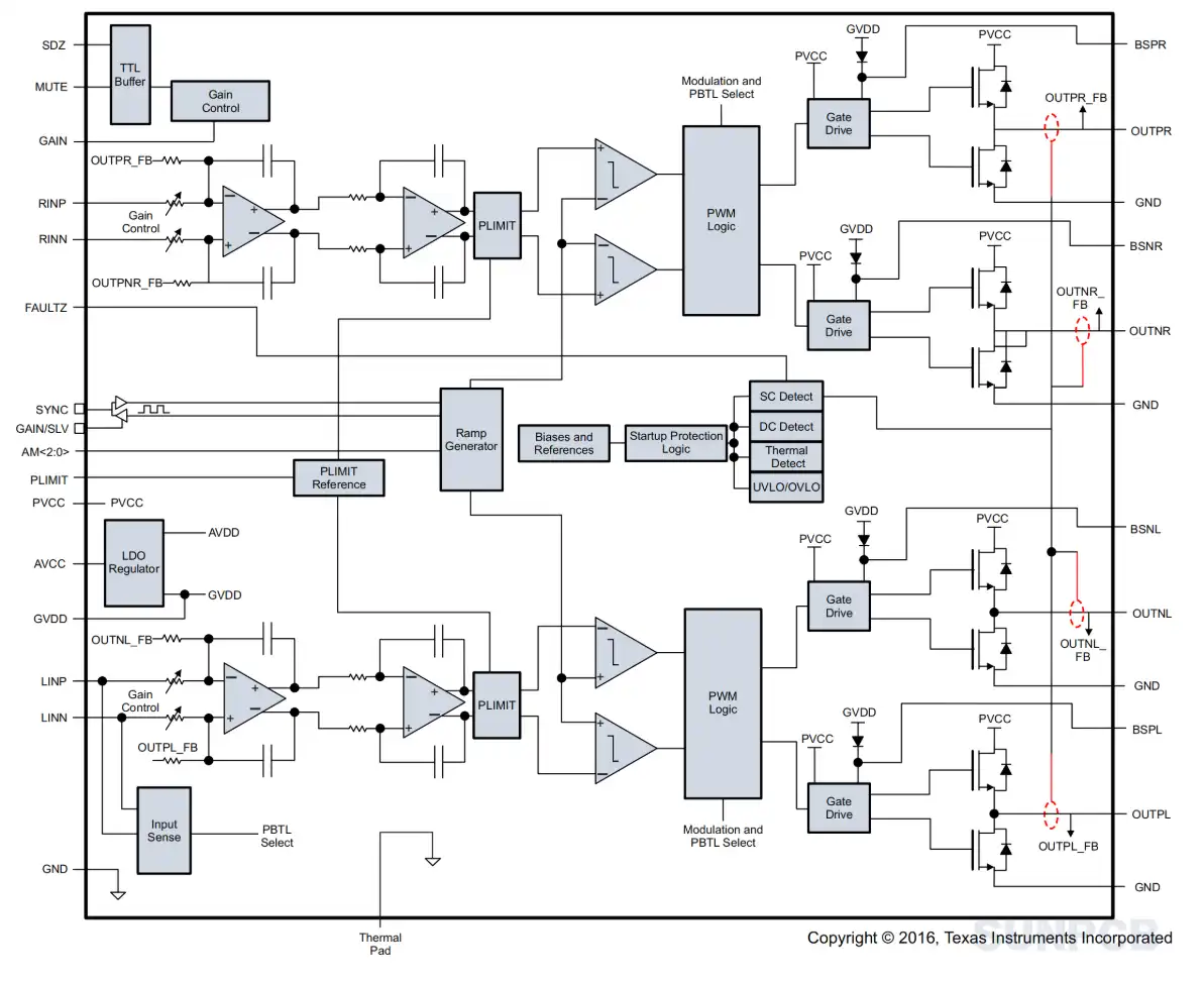
![]() TPA3116 functional block diagram pdf download (P13/P49)
TPA3116 functional block diagram pdf download (P13/P49)
- Input Stage: Handles differential and single-ended inputs.
- PWM Modulator: Converts audio signals to PWM for Class-D operation.
- Gate Drivers: Controls the power stage MOSFETs.
- Power Stage: Delivers high-efficiency output to speakers.
- Protection Circuits: Includes overvoltage, undervoltage, and thermal protection.
5. TPA3116 Texas Instruments Overview
5.1 Description
The TPA3116 is a stereo, efficient, Class-D amplifier for driving speakers up to 100 W/2 Ω in mono. It supports multiple configurations and high efficiency.
5.2 Overview
The TPA31xxD2 series are stereo efficient, digital amplifier power stage for driving speakers up to 100 W/2 Ω in mono. The high efficiency of the TPA3130D2 allows it to do 2 × 15 W without external heat sink on a single layer PCB. The TPA3118D2 can even run 2 × 30 W / 8 Ω without heat sink on a dual layer PCB. If even higher power is needed the TPA3116 does 2 × 50 W / 4 Ω with a small heatsink attached to its top side PowerPAD.
5.3 Features
- Supports multiple output configurations: 2 × 50 W (4 Ω, 21 V), 2 × 30 W (8 Ω, 24 V), 2 × 15 W (8 Ω, 15 V).
- Wide voltage range: 4.5 V to 26 V.
- >90% power efficiency reduces heat sink size.
- Advanced modulation schemes with AM avoidance.
- Up to 1.2-MHz switching frequency.
- Integrated self-protection circuits: overvoltage, undervoltage, overtemperature.
The TPA3116 pinout supports flexible configurations. Engineers should note the AM avoidance feature for clean audio output.
5.4 Applications
Mini-Micro Component; Speaker Bar; Docks; After-Market Automotive; CRT TV; Consumer Audio Applications
6. TPA3116 Package Dimension - HTSSOP-32
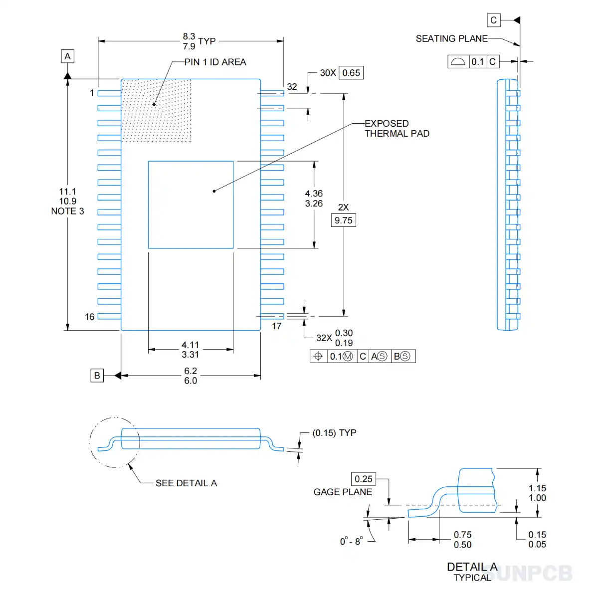
- Body dimensions: 11.00 mm × 6.20 mm.
- Thermal pad enhances heat dissipation.
- JEDEC MO-153 compliant.
7. TPA3116 Layout Example
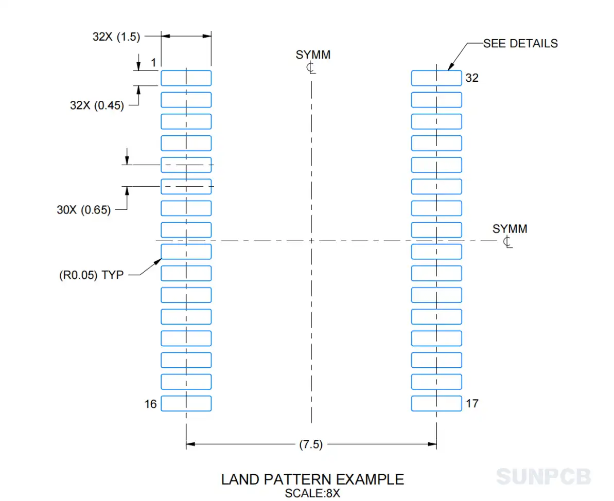
Image: TPA3116 Example Board Layout (Page 40/49)
![]() TPA3116 Layout (P40/P49)
TPA3116 Layout (P40/P49)
- Solder mask defined thermal pad.
- Recommended stencil thickness: 0.155 mm.
- Optimized for thermal performance.
8. TPA3116 Part Numbering System
| Part Number | Package | Body Size (Nominal) |
|---|---|---|
| TPA3116 | DAD (32) | 11.00 mm × 6.20 mm |
| TPA3118D2 | DAP (32) | 11.00 mm × 6.20 mm |
| TPA3130D2 | DAP (32) | 11.00 mm × 6.20 mm |
9. TPA3116 FAQs and Tips
Q: What is the maximum output power of TPA3116?
A: It delivers 2 × 50 W into 4 Ω at 21 V in BTL mode.
Q: Does TPA3116 require a heat sink?
A: A small heat sink is needed for 2 × 50 W operation.
Q: Can TPA3116 operate in mono mode?
A: Yes, it supports mono PBTL mode up to 100 W / 2 Ω.
Q: How to configure AM avoidance?
A: Set AM0, AM1, AM2 pins for desired switching frequency.
Q: What is the purpose of the PLIMIT pin?
A: It adjusts the power limit via a resistor divider from GVDD.
Q: Is the PowerPAD necessary?
A: Connect to GND for best thermal performance.
Q: What capacitors are needed for bootstrap pins?
A: Use 220 nF X5R capacitors for BSNL, BSNR, BSPL, BSPR.
Q: Can TPA3116 handle single-ended inputs?
A: Yes, it supports both differential and single-ended inputs.
Tips:
- Use decoupling capacitors to stabilize power supply.
- Ensure proper grounding to reduce noise.
- Check thermal design for high-power applications.
- Use X7R capacitors for GVDD decoupling.
- Verify output filter values for load impedance.