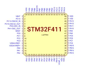
The STM32F103C8 is a versatile microcontroller from STMicroelectronics. Its pinout diagram and configuration are critical for engineers designing embedded systems. I’ve compiled key details, including the STM32F103C8 pinout diagram, to help you integrate this MCU effectively. Explore the STM32F103C8 pin configuration and schematics below.
1. STM32F103C8 Pinout Diagram
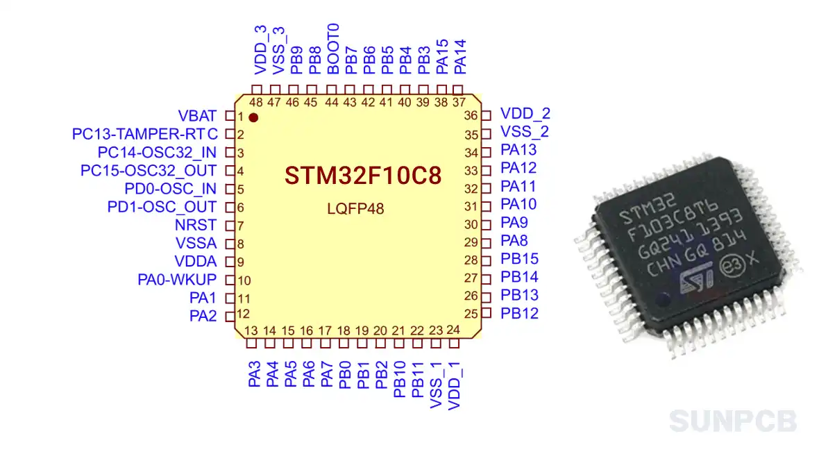
The STM32F103C8 pinout diagram shows the LQFP48 package layout. It’s essencial for connecting peripherals like STM32F103C8 ADC or STM32F103C8 USB. Check the PDF for detailed pin assignments.
2. STM32F103C8 Pin Configuration and Description
The STM32F103C8 pin configuration table lists all 48 pins. I’ve included pin numbers, names, types, and descriptions. Power pins and oscillator pins are in bold for clarity.
| Pin# | Pin Name | Type | I/O Level | Main Function | Pinout Description |
|---|---|---|---|---|---|
| 1 | VBAT | Power | - | Battery Supply | Powers RTC and backup registers. Connect to 1.8-3.6V. |
| 2 | PC13 | I/O | FT | GPIO | General-purpose I/O, 5V-tolerant. Can be used for STM32F103C8 external interrupt. |
| 3 | PC14 | I/O | FT | OSC32_IN | 32.768 kHz oscillator input. Connect to LSE crystal. |
| 4 | PC15 | I/O | FT | OSC32_OUT | 32.768 kHz oscillator output. Connect to LSE crystal. |
| 5 | PD0 | I/O | FT | GPIO | General-purpose I/O, 5V-tolerant. Supports STM32F103C8 CAN. |
| 6 | PD1 | I/O | FT | GPIO | General-purpose I/O, 5V-tolerant. Alternate function for CAN. |
| 7 | NRST | I | - | Reset | Active-low reset input. Connect to external reset circuit. |
| 8 | VSSA | Power | - | Analog Ground | Ground for analog circuits. Connect to system ground. |
| 9 | VDDA | Power | - | Analog Supply | 2.0-3.6V supply for ADC and analog circuits. |
| 10 | PA0 | I/O | FT | GPIO/ADC | General-purpose I/O or ADC input. Supports STM32F103C8 ADC. |
| 11 | PA1 | I/O | FT | GPIO/ADC | General-purpose I/O or ADC input. Used for STM32F103C8 timers. |
| 12 | PA2 | I/O | FT | GPIO/ADC | General-purpose I/O or ADC input. Supports STM32F103C8 PWM example. |
| 13 | PA3 | I/O | FT | GPIO/ADC | General-purpose I/O or ADC input. Alternate function for USART. |
| 14 | PA4 | I/O | FT | GPIO/ADC | General-purpose I/O or ADC input. Supports SPI. |
| 15 | PA5 | I/O | FT | GPIO/ADC | General-purpose I/O or ADC input. Used for SPI. |
| 16 | PA6 | I/O | FT | GPIO/ADC | General-purpose I/O or ADC input. Supports STM32F103C8 timers. |
| 17 | PA7 | I/O | FT | GPIO/ADC | General-purpose I/O or ADC input. Alternate function for SPI. |
| 18 | PB0 | I/O | FT | GPIO/ADC | General-purpose I/O or ADC input. Supports STM32F103C8 PWM example. |
| 19 | PB1 | I/O | FT | GPIO/ADC | General-purpose I/O or ADC input. Used for timers. |
| 20 | PB2 | I/O | FT | GPIO | General-purpose I/O, 5V-tolerant. Alternate function for boot. |
| 21 | PB10 | I/O | FT | GPIO | General-purpose I/O, 5V-tolerant. Supports STM32F103C8 I2C example. |
| 22 | PB11 | I/O | FT | GPIO | General-purpose I/O, 5V-tolerant. Used for I2C. |
| 23 | VSS_1 | Power | - | Ground | Digital ground. Connect to system ground. |
| 24 | VDD_1 | Power | - | Supply | 2.0-3.6V digital supply. Decouple with capacitors. |
| 25 | PB12 | I/O | FT | GPIO | General-purpose I/O, 5V-tolerant. Supports SPI and STM32F103C8 CAN. |
| 26 | PB13 | I/O | FT | GPIO | General-purpose I/O, 5V-tolerant. Used for SPI. |
| 27 | PB14 | I/O | FT | GPIO | General-purpose I/O, 5V-tolerant. Supports timers. |
| 28 | PB15 | I/O | FT | GPIO | General-purpose I/O, 5V-tolerant. Used for SPI. |
| 29 | PA8 | I/O | FT | GPIO | General-purpose I/O, 5V-tolerant. Supports STM32F103C8 timers. |
| 30 | PA9 | I/O | FT | GPIO | General-purpose I/O, 5V-tolerant. Used for USART. |
| 31 | PA10 | I/O | FT | GPIO | General-purpose I/O, 5V-tolerant. Supports USART. |
| 32 | PA11 | I/O | FT | GPIO | General-purpose I/O, 5V-tolerant. Supports STM32F103C8 USB. |
| 33 | PA12 | I/O | FT | GPIO | General-purpose I/O, 5V-tolerant. Used for STM32F103C8 USB. |
| 34 | PA13 | I/O | FT | JTMS/SWDIO | JTAG/SWD debug pin. 5V-tolerant. |
| 35 | VSS_2 | Power | - | Ground | Digital ground. Connect to system ground. |
| 36 | VDD_2 | Power | - | Supply | 2.0-3.6V digital supply. Decouple with capacitors. |
| 37 | PA14 | I/O | FT | JTCK/SWCLK | JTAG/SWD clock pin. 5V-tolerant. |
| 38 | PA15 | I/O | FT | JTDI | JTAG debug input. 5V-tolerant. |
| 39 | PB3 | I/O | FT | JTDO | JTAG debug output. 5V-tolerant. |
| 40 | PB4 | I/O | FT | JTRST | JTAG reset pin. 5V-tolerant. |
| 41 | PB5 | I/O | FT | GPIO | General-purpose I/O, 5V-tolerant. Supports STM32F103C8 I2C example. |
| 42 | PB6 | I/O | FT | GPIO | General-purpose I/O, 5V-tolerant. Used for I2C. |
| 43 | PB7 | I/O | FT | GPIO | General-purpose I/O, 5V-tolerant. Supports I2C. |
| 44 | BOOT0 | I | - | Boot Mode | Selects boot mode. Connect to ground or VDD. |
| 45 | PB8 | I/O | FT | GPIO | General-purpose I/O, 5V-tolerant. Supports STM32F103C8 timers. |
| 46 | PB9 | I/O | FT | GPIO | General-purpose I/O, 5V-tolerant. Used for CAN. |
| 47 | VSS_3 | Power | - | Ground | Digital ground. Connect to system ground. |
| 48 | VDD_3 | Power | - | Supply | 2.0-3.6V digital supply. Decouple with capacitors. |
3. STM32F103C8 Typical Application Circuit Diagram
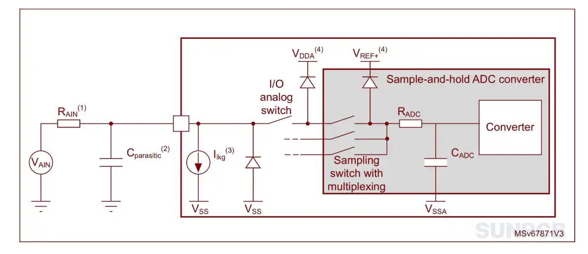
Image: STM32F103C8 Typical Application Circuit
The STM32F103C8 schematic shows a typical ADC connection. It includes decoupling capacitors and an external crystal. Engineers must ensure proper grounding and power decoupling. Use this STM32F103C8 circuit diagram for reliable ADC performance.
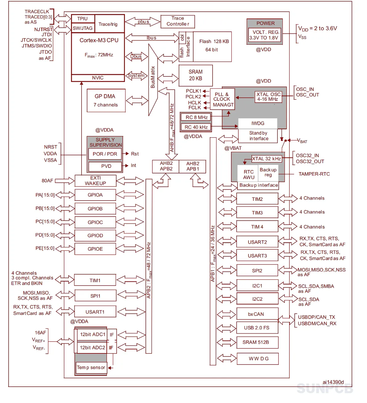
4. STM32F103C8 Functional Block Diagram
The STM32F103C8 block diagram highlights the MCU’s architecture. Key points include:
- Cortex-M3 Core: Drives high-performance processing.
- Flash Memory: Stores STM32F103C8 firmware.
- Peripheral Bus: Connects ADC, USB, and CAN.
- Timers: Enable STM32F103C8 PWM example.
![]() STM32F103C8 functional block diagram pdf download
STM32F103C8 functional block diagram pdf download
5. STM32F103C8 STMicroelectronics Overview
5.1 Description
The STM32F103C8 is a medium-density performance line MCU. It features a Cortex-M3 core and 64 KB Flash. I find it ideal for STM32F103C8 programming in embedded systems.
5.2 Overview
The STM32F103x8 and STM32F103xB microcontrollers operate in the –40 to +105 °C temperature range, at a 2.0 to 3.6 V power supply. A comprehensive set of power-saving modes allows the design of low-power applications. The STM32F103x8 and STM32F103xB incorporate a high-performance ARM Cortex-M3 32-bit RISC core operating at a 72 MHz frequency, high-speed embedded memories (Flash memory up to 128 Kbytes and SRAM up to 20 Kbytes), and an extensive range of enhanced I/Os and peripherals connected to two APB buses. All devices offer two 12-bit ADCs, three general-purpose 16-bit timers plus one PWM timer, as well as standard and advanced communication interfaces: up to two I2Cs and SPIs, three USARTs, an USB and a CAN.
5.3 Features
- Arm 32-bit Cortex-M3 CPU core
- 72 MHz maximum frequency, 1.25 DMIPS/MHz
- 64 or 128 Kbytes of Flash memory
- 20 Kbytes of SRAM
- 2.0 to 3.6 V application supply
- 4 to 16 MHz crystal oscillator
- Two 12-bit, 1 µs A/D converters (up to 16 channels)
- 7-channel DMA controller
- Up to 80 fast I/O ports
- Seven timers
- Up to nine communication interfaces (I2C, USART, SPI, CAN, USB)
These features make the STM32F103C8 versatile. Engineers should note the STM32F103C8 timers and STM32F103C8 USB bootloader for advanced applications.
5.4 Applications
Motor drives; Application control; Medical equipment; Industrial applications; PLC; Inverters; Printers; Scanners; Alarm systems; Video intercom; HVAC
6. STM32F103C8 Part Numbering System
The STM32F103C8 pin diagram is part of the STM32 family. The ordering information (Page 104) defines the part numbering.
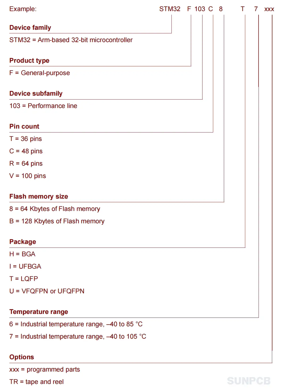
| Field | Value | Description |
|---|---|---|
| Device Family | STM32 | Arm-based 32-bit microcontroller |
| Product Type | F | General-purpose |
| Device Subfamily | 103 | Performance line |
| Pin Count | C | 48 pins |
| Flash Memory Size | 8 | 64 Kbytes of Flash memory |
| Package | T | LQFP |
| Temperature Range | 6 or 7 | 6: -40 to 85°C; 7: -40 to 105°C |
7. STM32F103C8 FAQs and Tips
FAQs
Q: How do I configure the STM32F103C8 ADC?
A: The ADC needs proper pin setup. Use PA0-PA7 or PB0-PB1. Enable the ADC clock in RCC. I’ve set it up for STM32F103C8 ADC in single-conversion mode. Check the reference manual.
Q: Can I use the STM32F103C8 USB without external crystal?
A: No, USB requires a precise clock. Use an 8 MHz crystal on OSC_IN/OSC_OUT. I learned this when testing STM32F103C8 USB driver.
Q: How to program the STM32F103C8?
A: Use SWD or JTAG. Connect PA13, PA14, and PB3-PB4. Tools like STM32CubeIDE work well. I use STM32F103C8 programming with ST-LINK.
Q: What’s the max clock speed for STM32F103C8?
A: It’s 72 MHz. Configure the PLL correctly. Overclocking isn’t recomended.
Q: How to use STM32F103C8 I2C?
A: Use PB6-PB7 or PB10-PB11. Enable I2C clock and set pull-up resistors. I’ve coded STM32F103C8 I2C example for sensors.
Q: Does STM32F103C8 support CAN?
A: Yes, use PB8-PB9 or PD0-PD1. Enable CAN clock and add a transceiver. It’s great for STM32F103C8 CAN networks.
Q: How to set up STM32F103C8 timers?
A: Enable TIM1-TIM4 in RCC. Configure PA8, PB6, etc., for PWM. I’ve used STM32F103C8 generic timer for motor control.
Q: What’s the STM32F103C8 flash size?
A: It has 64 KB Flash. Enough for most STM32F103C8 firmware. Plan memory usage carefully.
Tips
1. Decoupling Capacitors: Always add 100 nF capacitors near VDD pins. I had noise issues without them.
2. Crystal Selection: Use an 8 MHz crystal for USB stability. It’s critical for STM32F103C8 USB.
3. Boot Mode: Set BOOT0 to 0 for Flash boot. I forgot this once and debugged for hours.
4. ADC Calibration: Run ADC calibration before use. It improves ADC accuracy in STM32F103C8.
5. Low-Power Modes: Use Sleep or Stop mode to save power. I optimized battery life with low-power settings.
6. SWD Debugging: Reserve PA13-PA14 for SWD. It simplifies STM32F103C8 programming.